• APT50GH120BSC20 Power Module: Latest Performance Report

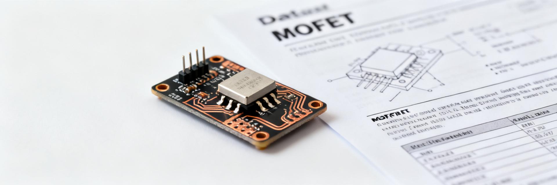
    Point: The APT50GH120BSC20 is presented by the manufacturer as a 1200 V, 50 A Fast Field‑Stop IGBT paired with an integrated SiC diode in a TO‑247 package; this report consolidates datasheet curves, lab benchmarking approaches, and practical design guidance to evaluate real‑world performance. Evidence: Microchip’s published datasheet provides the core VCE, switching energy, thermal impedance and SOA curves used throughout this analysis. Explanation: The goal is to give power electronics engineers, design leads, and procurement teams a concise, data driven assessment of whether the APT50GH120BSC20 meets modern high‑power switching needs and what to test first. Link: Refer to the Microchip datasheet for raw curves and recommended limits for further validation. Point: This report covers device background, electrical and thermal performance, recommended test methodology, integration practices, and market positioning to enable rapid evaluation. Evidence: Sections mirror standard qualification flows used in bench characterization and system integration. Explanation: Readers will gain actionable KPIs (Eon/Eoff, conduction loss, Zth), step‑by‑step test setups, and a short checklist for selection or prototype procurement. Link: Use the datasheet figures as the baseline for comparisons and for parameter extraction. 1 — Background & Device Overview (Background) 1.1 Device specifications summary Point: Key electrical and mechanical specifications define the integration envelope for the APT50GH120BSC20. Evidence: Manufacturer datasheet lists the following nominal values and limits. Explanation: The table below summarizes the primary specs engineers use during initial selection and thermal budgeting. Link: All values are consistent with the Microchip datasheet and should be cross‑checked against the actual lot release data. ParameterValue / Note Voltage rating1200 V (blocking) Current rating50 A (continuous, case temp limited) PackageTO‑247 TopologyFast Field‑Stop IGBT + integrated SiC diode Max junction temperatureTypically 150 °C (see datasheet limit) 1.2 Architecture & key features Point: The field‑stop IGBT structure reduces tail charge and improves turn‑off speed versus conventional IGBTs, and the integrated SiC diode reduces reverse recovery losses. Evidence: Datasheet switching curves show reduced Eoff and improved dV/dt tolerance compared to legacy designs. Explanation: In practice, the field‑stop doping profile shortens minority‑carrier lifetime during turn‑off leading to lower switching energy, while the SiC diode’s limited recovery current reduces diode‑related switching spikes; together these traits improve converter efficiency at medium‑to‑high frequencies. Link: Confirm specific Eon/Eoff tradeoffs on the datasheet switching energy plots when defining gate drive and snubber strategy. 1.3 Typical applications & target markets Point: The device targets traction inverters, solar and battery inverters, motor drives and UPS systems where 1200 V blocking and 50 A capability are typical. Evidence: Application notes and datasheet suggested use cases highlight traction and industrial drives. Explanation: For traction and high‑power motor drives the device’s reduced switching losses and robust diode recovery are advantageous at switching frequencies in the single‑ to low‑tens of kHz range; for solar inverters the thermal and SOA margins dictate cooling designs. Link: Use the datasheet’s thermal and SOA charts to match application duty cycles and switching frequency requirements. 2 — Electrical Performance Analysis (Data) 2.1 Switching characteristics (turn‑on/turn‑off) Point: Important switching metrics to measure are rise/fall times (tr, tf), turn‑on/turn‑off delay (tq), dV/dt, gate charge and energy per event (Eon, Eoff)—these determine converter switching loss per kHz. Evidence: Datasheet switching energy curves provide Eon/Eoff vs. Ic and VCE conditions which are the reference for lab verification. Explanation: In bench tests, expect datasheet Eon/Eoff to be a best‑case measured at specific gate resistances and inductance; parasitic inductance, gate drive impedance, and measurement clamp networks will typically increase measured energy by 10–30%. Suggested figure: capture switching waveforms (VCE, IC, VGE) with ≥200 MHz oscilloscope bandwidth and appropriately rated current probes to resolve di/dt and dV/dt transients. Link: Use the datasheet switching waveform conditions to reproduce comparable bench setups. 2.2 Conduction behavior & losses Point: Conduction loss is dominated by VCE(sat) across Ic and temperature; quantify Pcond = VCE(sat) × Ic averaged over the conduction interval. Evidence: Manufacturer VCE vs Ic curves and temperature coefficients show VCE rise with junction temperature. Explanation: Example calculation — assuming VCE(sat) = 1.2 V at 25 °C and 1.6 V at 125 °C at Ic = 50 A: Pcond@25 °C = 1.2 V × 50 A = 60 W; Pcond@125 °C = 1.6 V × 50 A = 80 W. This 33% increase highlights the impact of thermal derating on steady losses and the importance of keeping junction temperature low. Link: Cross‑reference the datasheet conduction curves and temperature coefficients when modeling inverter losses. 2.3 Dynamic behavior under transient loads Point: Short‑circuit withstand, unclamped inductive switching behavior and SOA margins determine robustness under faults and transients. Evidence: Datasheet provides transient thermal impedance Zth(j‑c) vs time and SOA boundaries for pulsed conditions. Explanation: Use Zth(j‑c) to convert pulse energy into delta‑Tj for short pulses (e.g., 100 µs–10 ms); likewise, ensure unclamped inductive switching events do not exceed the instantaneous SOA or the diode avalanche limits. Practical bench validation should include single‑pulse and repetitive pulse sequences to map real thermal response against datasheet curves. Link: Validate with the datasheet’s transient Zth plots and SOA diagrams before qualifying a design for field deployment. 3 — Thermal Performance & Reliability (Data) 3.1 Thermal impedance and cooling requirements Point: Thermal design requires understanding both steady‑state Rth(j‑c)/Rth(c‑a) and transient Zth for pulsed loads. Evidence: Datasheet lists junction‑to‑case Rth and Zth(j‑c) vs pulse duration. Explanation: For continuous operation, compute required heatsink thermal resistance: Rth_required = (Tj_max − Tamb − P×Rth_case‑sink)/(P), where P is total dissipated power. For example, a 60 W steady loss and 100 °C max junction yields a required overall thermal path to limit ambient rise; forced convection or a dedicated heatsink plate is typically necessary for 50 A continuous use in TO‑247. Link: Use the datasheet Rth and Zth curves to size heatsinks and cooling fans for your duty cycle. 3.2 Lifetime & derating guidelines Point: Continuous operation near Tmax accelerates wear mechanisms; conservative derating extends lifetime. Evidence: Datasheet recommended maximum junction temperatures and derating notes provide acceptable operating envelopes. Explanation: Practical derating: for continuous operation target 3.3 Failure modes & reliability testing to prioritize Point: Typical failure modes include bond lift, gate oxide breakdown, and diode avalanche or thermal runaway; prioritize tests accordingly. Evidence: Industry reliability data for field‑stop IGBTs and SiC diodes show prevalence of bond wire fatigue under thermal cycling and oxide degradation under repetitive VGE stress. Explanation: Recommended tests: power cycling (to stress bond wires and solder interfaces), thermal shock, gate overstress, and avalanche/short‑circuit endurance; include statistical sampling to establish mean cycles to failure. Link: Correlate failure signatures from testing against datasheet SOA and transient limits to refine system protections. 4 — Benchmarking & Test Methodology (Method) 4.1 Recommended test setups & measurement points Point: Standardized switching test schematics improve repeatability and traceability when comparing devices. Evidence: Typical switching bench uses a clamp diode, inductive load, VDC source, gate driver with adjustable Rg, and measurement nodes at VCE, IC and VGE. Explanation: Critical measurement specs: oscilloscope ≥200 MHz (preferably 500 MHz for sharp edges), current probe bandwidth matching di/dt, and low‑inductance measurement leads. Place voltage probes close to the device terminals and minimize loop inductance to avoid measurement artifacts. Link: Reproduce the datasheet’s test conditions (Vdc, gate drive, Lload) to validate your bench against published curves. 4.2 Repeatable procedures for electrical & thermal tests Point: Define step‑by‑step procedures and environmental controls to ensure comparable results. Evidence: Repeatability improves when ambient temperature and drive conditions are tightly controlled and when sample size is sufficient. Explanation: Procedure highlights: stabilize ambient at 25 ±2 °C for electrical tests, use a minimum of 5 samples for statistical confidence, document Vdc, Ic, switching frequency and gate resistor. For thermal tests, allow steady‑state to settle and log junction (or case) temperatures with calibrated sensors. Link: Standardize reporting format to include raw waveform captures, test conditions, and sample statistics. 4.3 Data analysis templates & KPIs Point: Key KPIs to extract are Eon, Eoff, Qg, total switching loss per kHz, conduction loss at defined temperatures, thermal rise per watt, and SOA margin. Evidence: Plotting Eon/Eoff vs Ic and loss vs switching frequency provides immediate comparisons across devices. Explanation: Recommended outputs: switching energy tables, loss vs current charts, normalized efficiency vs frequency curves, and a thermal map for typical duty cycles. These deliverables enable rapid tradeoff decisions for BOM and cooling design. Link: Use the datasheet curves as a reference baseline when filling templates. 5 — Design Integration & Practical Recommendations (Method/Action) 5.1 Gate drive and protection recommendations Point: Proper gate drive selection and active protection are critical for achieving the datasheet performance in system contexts. Evidence: Datasheet gate charge and recommended VGE limits set the acceptable drive window. Explanation: Suggested practices: pick gate resistance to balance dv/dt and switching loss (start with Rg ~5–10 Ω for bench tuning), implement Miller clamp or active turn‑off to prevent spurious turn‑on, and include desaturation detection with timed shutdown for short‑circuit protection. Ensure gate drive isolation and common‑mode transient immunity are specified for your system voltage environment. Link: Verify drive levels against the datasheet’s recommended VGE(max/min) and charge curves. 5.2 PCB layout, package mounting & cooling best practices Point: Mechanical mounting, thermal interface materials (TIM), and PCB copper influence thermal performance significantly for TO‑247 parts. Evidence: Thermal contact resistance and clamping torque directly affect junction‑to‑case and case‑to‑heatsink conduction. Explanation: Best practices: use recommended torque for mounting screws, thin but thermally conductive TIM to minimize interface resistance, large copper pour on the case underside if applicable, and thermal vias to spread heat on multi‑layer boards. For high duty cycles, prefer direct clamping to a heatsink plate and forced convection. Link: Cross‑check mounting torque and TIM specs with the manufacturer’s assembly notes in the datasheet. 5.3 System‑level protections & EMI/ snubber strategies Point: Snubber topology and EMI mitigation will affect both performance and regulatory compliance. Evidence: Datasheet switching transients indicate expected dV/dt and di/dt ranges which inform snubber selection. Explanation: For high switching speed, RCD snubbers limit voltage spikes and clamp energy with modest power dissipation; RC snubbers reduce dv/dt but incur continuous losses. Use common‑mode chokes, proper decoupling bank placement near DC link, and minimize loop area to reduce radiated EMI. Balance snubber losses against switching loss improvements to find the optimal tradeoff. Link: Use datasheet transient figures to size snubber components conservatively. 6 — Comparative Case Study & Market Positioning (Case) 6.1 Head‑to‑head comparison vs comparable 1200 V / 50 A devices Point: Engineers must compare switching loss, conduction loss, thermal impedance, package and supply chain factors across vendors. Evidence: Benchmarked KPIs (Eoff, VCE(sat), Rth) are primary differentiators in similar packages. Explanation: A concise comparative table (below) should include the APT50GH120BSC20 alongside two comparable devices from major vendors, listing Eon/Eoff at a representative Ic, VCE(sat) at 25/125 °C, and Rth(j‑c). This allows quick prioritization based on system‑level efficiency or thermal constraints. Link: Use datasheet numbers as a baseline and validate with bench measurements before final selection. DeviceEoff @ 50 A (mJ)VCE(sat) @50 A (V)Rth(j‑c) (°C/W) APT50GH120BSC20Refer to datasheet curveRefer to datasheet curveRefer to datasheet Competitor A (1200 V / 50 A)Bench value neededBench value neededBench value needed Competitor B (1200 V / 50 A)Bench value neededBench value neededBench value needed 6.2 Cost vs performance tradeoffs and BOM impact Point: Device selection impacts system efficiency, cooling requirements and overall BOM cost. Evidence: Higher performing parts can reduce heatsink size or fan power, offsetting higher unit cost over system lifetime. Explanation: Example TCO scenario: a 1% system efficiency improvement at full load for a 10 kW motor drive can translate to significant annual energy savings; weigh that against incremental device cost and any additional required board space or snubbing components. Early prototyping should quantify these tradeoffs with measured loss curves. Link: Use the benchmarking KPIs to populate a BOM impact model for your product. 6.3 Selection checklist for engineers Point: A short checklist accelerates go/no‑go decisions for prototypes and procurement. Evidence: Practical factors include voltage/current margins, switching frequency, thermal budget, SOA needs, and supply risk. Explanation: Recommend using a checklist that captures required Vdc margin, peak and RMS currents, expected switching frequency, cooling capacity, lifetime targets, and acceptable unit cost. If the design demands moderate switching frequency (≤20 kHz) with a focus on reduced diode recovery loss, the device’s Fast Field‑Stop IGBT plus SiC diode is a strong candidate. Link: Validate checklist entries against datasheet limits and bench test results. Conclusion Point: The APT50GH120BSC20 demonstrates attributes—Fast Field‑Stop switching and an integrated SiC diode—that make it a compelling Power Module option for many medium‑power converters seeking improved efficiency and reduced diode recovery losses. Evidence: Datasheet switching and thermal curves indicate competitive Eon/Eoff and thermal impedance characteristics, with recommended limits for continuous and pulsed operation. Explanation: For engineers designing traction inverters, motor drives or inverters where switching Performance and thermal management are primary concerns, this part is worth prototype evaluation; primary caveats are the need for careful thermal design and conservative derating for continuous 50 A operation. Link: Begin with the benchmark procedures and thermal checks recommended above and confirm with the Microchip datasheet during prototype testing. Key Summary Fast Field‑Stop IGBT plus integrated SiC diode offers reduced switching and recovery losses, improving converter efficiency when switching Performance matters; validate with Eon/Eoff bench tests. Thermal design is critical: conduction losses increase significantly with temperature—expect ~30% higher conduction loss at high junction temperature for typical VCE(sat) shifts. Benchmark using standardized test setups (defined Vdc, Rg, Lload) and extract KPIs (Eon/Eoff, Qg, Rth/Zth, SOA margin) to inform BOM and cooling tradeoffs. Gate drive, snubber and PCB layout decisions materially affect measured Performance—optimize Rg, minimize loop inductance, and apply appropriate snubber topology. Use the datasheet as the baseline for initial selection, then confirm with sample‑level testing for production readiness and reliability assurance. Frequently Asked Questions What are the key switching loss characteristics of the APT50GH120BSC20? The APT50GH120BSC20’s switching loss characteristics are defined by datasheet Eon and Eoff curves which should be reproduced on the bench using the same Vdc, gate drive, and load inductance conditions. Practical measurements often show 10–30% higher energy due to parasitics; therefore, engineers should capture switching waveforms with high‑bandwidth probes and account for board inductance when estimating converter switching Performance. How should engineers size cooling for continuous 50 A operation of the APT50GH120BSC20? Cooling sizing begins with total dissipated power (conduction + switching). Use the datasheet Rth(j‑c) and Zth for pulse behavior to compute allowable thermal path; for 50 A continuous example, anticipate steady conduction losses on the order of tens of watts and size heatsink/fan to keep Tj below conservative limits (e.g., target ≤125 °C). Validate with thermal sensors and account for case‑to‑heatsink interface resistance. Is the APT50GH120BSC20 suitable for high‑frequency motor drive applications in terms of Performance? The integrated SiC diode and field‑stop IGBT reduce diode recovery and turn‑off losses, making the device suitable for moderate switching frequencies (single‑ to low‑tens of kHz). For very high switching frequencies, evaluate total loss (switching + conduction) against competing devices and verify thermal capability; perform bench Eon/Eoff and temperature‑rise tests to confirm system‑level Performance.
  • APT50GH120B Datasheet Deep Dive: Specs, Ratings & Curves

    The APT50GH120B datasheet opens with a striking set of headline specifications that frame its use in power-conversion designs: a 1200 V collector-emitter rating, a 50 A nominal collector current, Fast Field‑Stop IGBT topology, and an indicated device power dissipation (Pd) that implies robust thermal handling up to elevated case/junction temperatures. These numbers—drawn from the official manufacturer datasheet—set expectations for inverters, motor drives and UPS applications where high blocking voltage and moderate current capability are required. This article’s purpose is practical and actionable: to walk an engineer through the APT50GH120B datasheet so they can interpret absolute ratings, translate thermal and switching curves into real-world loss and heatsink calculations, verify safe operating area margins, and run the critical bench tests needed before production. Where numeric claims are used, they reference the official Microchip datasheet figures and recommended test conditions; readers are encouraged to consult the manufacturer PDF for plotted curves and raw tables. The approach is US-market pragmatic—showing worked examples for switching-loss estimation and thermal sizing so the datasheet becomes a usable design tool rather than just a reference sheet. 1 — Product overview & quick spec summary (background) Key device identity and family position Point: The APT50GH120B is a Fast Field‑Stop IGBT rated for 1200 V VCES and specified for nominal 50 A continuous collector current in standard test conditions, positioned as a mid‑power member of Microchip’s 1200 V product line. Evidence: The device is listed in the official manufacturer datasheet as a Fast Field‑Stop IGBT with the stated voltage and current ratings and typical package options. Explanation: Fast Field‑Stop IGBT topology delivers a balance between conduction efficiency and improved turn‑off capability compared with older soft‑recovery IGBTs, making this part suitable for three‑phase inverter half‑bridges, motor drives up to the tens of kilowatts range, and uninterruptible power supplies where switching frequency and thermal robustness matter. Link: For exact package codes, ordering information and full curve sets, consult the official manufacturer datasheet. At-a-glance electrical & thermal highlights Point: Key electrical and thermal callouts include VCES = 1200 V, gate‑emitter limits typically ±20 V, on‑state VCE(sat) scaling with IC, and thermal resistances Rth(j‑c) reported per package with Pd and Tc/Ta test conditions. Evidence: The datasheet provides tabulated DC characteristics (VCE(sat), VGE(th), IC‑dependant leakage) and thermal tables showing Rth(j‑c) and maximum allowable junction temperatures. Explanation: Practical design must note the device’s Pd and maximum rated junction temperature—datasheet figures show generous thermal allowance (Pd and high Tj limits), but the real constraint is case‑to‑ambient path and heatsinking; a claim of high Pd is useful only if the board and heatsink deliver low Rth(c‑a). Also watch for any datasheet “red flags” such as elevated leakage at high temperature or restrictive VGE limits—these affect standby losses and driver design. Link: See the manufacturer datasheet for the numerical Rth values and temperature dependence charts. Typical application block & recommended use-cases Point: Best‑fit applications include inverter half‑bridges for motors, traction or industrial drives, PFC stages with 1200 V needs, and UPS inverter legs, with constraints arising mainly from thermal dissipation and SOA for hard‑switching duties. Evidence: The datasheet positions the device for inverter and drive use and supplies switching energy curves and SOA plots tailored to these roles. Explanation: For motor drives, prioritize low VCE(sat) and switching energy at the intended switching frequency; for PFC, prioritize low switching losses during high‑frequency operation and ensure the part’s capacitances and gate charge are compatible with the chosen driver. Device package and mounting options in the datasheet determine mechanical and thermal implementation choices on the heatsink or busbar. Link: The manufacturer datasheet includes recommended application schematics and typical connection diagrams to follow. 2 — Absolute maximum ratings & thermal limits (data analysis) Interpreting absolute max tables Point: Absolute maximum tables list the non‑recoverable limits (VCES, VGE, IC peak, ICM, junction temperature) under defined conditions—understanding test conditions (Tc vs Ta) is essential to avoid misinterpretation. Evidence: The datasheet separates ratings measured at a fixed case temperature (Tc = 25°C) from those at ambient (Ta) and clarifies pulsed vs continuous values. Explanation: “Absolute max” means the part must not be exposed to those conditions even transiently without risking irreversible damage; in contrast “recommended operating” limits add safety margins and duty constraints. For instance, a pulsed ICM may be much higher than continuous IC but depends strictly on specified pulse width and repetition period. Designers should translate pulsed-limit numbers into permissible short‑duration events (for example, startup inrush or fault clearing) using the datasheet’s pulse width and thermal transient guidance. Link: Refer to the absolute maximum ratings section of the official datasheet for exact pulse durations and repetition rules. Thermal resistances, mounting assumptions, and heat-sinking Point: Thermal resistance values—Rth(j‑c), Rth(c‑a) when provided, and Pd—are the bridge between electrical loss and temperature rise; use them to size heatsinks and confirm junction limits. Evidence: The datasheet provides Rth(j‑c) per package and specifies test conditions (cold plate vs. free air) that define stated Pd values. Explanation: Use a simple thermal model: Tj = Tc + Pd × Rth(j‑c). Example: if steady‑state dissipated power Pd_device = 10 W and Rth(j‑c) = 0.4 °C/W, junction rise over case = 4 °C; if case is kept at 75 °C, Tj = 79 °C. For board‑level or free‑air cases, include Rth(c‑a) or heatsink thermal resistance: Tj = Ta + Pd × (Rth(c‑a) + Rth(j‑c)). Always add margin—datasheet test conditions assume ideal mounting; real assemblies add thermal interfaces, TIMs, and thermal grease impact. Link: Use the manufacturer datasheet thermal tables and mounting notes when performing these calculations. Safe operating area (SOA) and short-circuit behavior Point: SOA plots define allowable combinations of VCE and IC for dc and pulsed operations and indicate the device’s short‑circuit robustness and thermal limits under surge conditions. Evidence: The datasheet includes SOA graphs showing single‑pulse, repetitive‑pulse and thermal‑limited continuous regions, plus short‑circuit withstand time under defined gate drive and supply conditions. Explanation: Interpret SOA by aligning your expected switching stress—peak VCE during turn‑off and collector current—against the SOA envelope at the appropriate pulse width and duty. For short‑circuit events, datasheet short‑circuit curves typically show the maximum duration the device can survive under specified VCC, IC, Rg and cooling; use these to set protection trip times (e.g., desaturation detection or fast current limit). If the device’s SOA margin is slim at your intended operating point, consider paralleling devices judiciously or selecting a higher‑SOA part. Link: Consult the official datasheet SOA and short‑circuit sections to extract pulse‑width dependent limits. 3 — Electrical characteristics & dynamic/switching curves (data analysis) DC characteristics: VCE(sat), leakage, gate threshold, transconductance Point: DC tables enable conduction‑loss estimation and standby loss budgeting—VCE(sat) vs. IC and temperature governs on‑state conduction loss while leakage vs. Tj determines off‑state standby losses. Evidence: The datasheet provides VCE(sat) curves across collector current and temperature, gate threshold (VGE(th)) ranges, and typical leakage currents at rated VCES and elevated temperatures. Explanation: For conduction loss: Pcond ≈ IC × VCE(sat) (for a single device in conduction). Example: at IC = 25 A and VCE(sat) = 1.0 V, conduction loss per device is 25 W. Leakage current rising exponentially with Tj can dominate no‑load or low‑duty applications; quantify worst‑case leakage at maximum junction temperature from the datasheet and include it in thermal budgeting. Transconductance and VGE(th) ranges guide gate drive margin selection—ensure VGE drive amplitude yields sufficient VCE(sat) while staying within VGE(max). Link: Use the manufacturer’s DC characteristic plots to pull the specific VCE(sat) and leakage numbers for your operating points. Switching energy, turn-on/turn-off curves and driver implications Point: Esw curves (Eon, Eoff) quantify energy dissipated per switching transition and are the core input for switching‑loss estimates; they are measured under specified test conditions that must match your driver and Rg to be directly usable. Evidence: The datasheet offers Eon/Eoff vs. IC plots for given VCC and gate resistor (Rg) values, and shows typical current and voltage waveforms. Explanation: To estimate switching losses, use Pswitch = (Eon + Eoff) × fsw where fsw is switching frequency. Worked example: if combined Esw = 0.25 J per switching cycle at your operating IC/VCC and fsw = 10 kHz, switching loss = 0.25 J × 10,000 = 2500 W (per device) — clearly indicating conditions where a different operating point or device is required. Note that datasheet Esw is sensitive to gate resistance, stray inductance, and dV/dt; always align your driver Rg and layout to the test conditions or re‑measure in the lab. Link: The manufacturer datasheet’s switching‑energy plots list the exact Rg and VCC used for each curve. Capacitances, Miller effect and gate drive recommendations Point: Cies, Cres and Coss define the gate charge behavior and Miller plateau dynamics; large Miller capacitance increases gate charge and slows dv/dt for a given driver, affecting switching losses and EMI. Evidence: The datasheet provides capacitance measurements at specified VCE bias points and gate charge Qg or Miller charge Qgd figures for typical voltages. Explanation: Use the provided Qg and Qgd to size gate drivers: driver peak current must supply Qg during the desired transition time. For example, to achieve a gate transition in 100 ns with Qg = 60 nC requires average gate current I = Qg / t = 0.6 A. Gate resistor recommendations in the datasheet (typical Rg range) are a starting point; choose Rg to balance dv/dt control (reduce ringing and EMI) and acceptable switching‑loss increase. Also watch the Miller plateau voltage when designing active Miller suppression or desat protection in the driver. Link: See datasheet capacitance and gate‑charge tables for numeric Qg/Qgd values under test conditions. 4 — Electrical ratings in system context: derating & reliability (method/guidelines) Derating rules: temperature, frequency, and package constraints Point: Derating current or power with temperature is mandatory—apply linear or piecewise reductions using datasheet derating curves and thermal limits to maintain reliability. Evidence: The datasheet includes current or power derating curves referenced to case temperature or ambient temperature with mounting conditions spelled out. Explanation: A practical rule‑of‑thumb derived from typical datasheet behavior: reduce continuous current by about 10–20% for every 25 °C rise in junction or case temperature beyond nominal test conditions (exact percent varies by package and must be taken from the datasheet). For switching frequency, increase margin as Esw × fsw contributes directly to Pd. Implement a derating table in your thermal budget: list worst‑case ambient, expected Pd (conduction + switching + leakage), heatsink Rth and resulting Tj, then apply conservative derating to set allowable continuous current. Link: Use the manufacturer’s derating curves to derive exact percent reductions for your package and mounting. Lifetime, SOA margins and safe design practices Point: Long‑term reliability depends on thermal cycling amplitude, Tj,max headroom and SOA margins; set conservative maximum junction temperatures and aim for lower thermal swing to minimize thermal fatigue. Evidence: The datasheet and related application notes discuss maximum junction temperatures and suggested operating regions for long life. Explanation: Practical guidance: set design Tj,max at least 10–20 °C below datasheet absolute maximum for continuous operation to allow for transient events, measurement uncertainties and aging. Reduce thermal cycle amplitude (ΔTj) to limit solder and die‑attach fatigue; where possible, use snubbers or soft‑switching techniques to reduce peak stress. Include an SOA margin factor (e.g., 20–30%) when sizing for worst‑case transient currents to avoid operating on the edge of the SOA envelope. Link: Consult the datasheet SOA and thermal guidance to quantify margins for your application. Testing & validation checklist for prototypes Point: A structured prototype validation plan prevents late failures—focus on thermal imaging, switching energy verification, and short‑circuit robustness aligned with datasheet test conditions. Evidence: The datasheet provides reference test circuits and conditions for switching‑energy, SOA and short‑circuit measurements that should be replicated in the lab. Explanation: Recommended tests: 1) steady‑state thermal imaging under representative load to verify predicted Tj and hotspot locations; 2) switching loss validation by measuring VCE and IC waveforms with known Rg and layout to compute Esw and compare to datasheet curves; 3) controlled short‑circuit tests to confirm protection trip times and device survival within the datasheet’s short‑circuit withstand limits. Record exact test conditions (VCC, IC, Rg, ambient, heatsink), and compare measured results to datasheet numbers to validate assumptions. Link: Follow the test circuits and notes in the official datasheet when setting up these measurements. 5 — Application examples, comparisons & troubleshooting (case study) Example: inverter half-bridge design with APT50GH120B Point: Designing a half‑bridge requires choosing gate resistor, snubber, heatsink and computing steady‑state losses from both conduction and switching components. Evidence: Datasheet figures for VCE(sat), Esw and capacitances supply inputs for these calculations. Explanation and worked example: assume a three‑phase inverter where each device conducts an RMS current of 20 A, switching at 8 kHz with combined Esw per cycle (Eon+Eoff) of 0.08 J at test conditions approximating your driver. Conduction loss (approx): Pcond = IC_rms × VCE(sat_avg). If VCE(sat_avg) ≈ 1.1 V at 20 A, Pcond ≈ 22 W. Switching loss = 0.08 J × 8000 = 640 W — indicating switching dominates and you must either reduce Esw via optimized gate drive/Rg or lower switching frequency. Select Rg to match datasheet test Rg baseline, add RC snubber sized to clamp peak VCE within SOA margins, and size heatsink by summing Pd_total and using Rth(j‑c) from datasheet to keep Tj below chosen headroom. Link: Use the datasheet’s switching and conduction curves to refine these numbers for your exact conditions. Comparing APT50GH120B to nearby parts (benchmarks) Point: Compare on‑state voltage, Esw, and thermal ratings when evaluating alternatives; motor drives often prioritize low VCE(sat) and moderate Esw, whereas PFC may prioritize low Esw at high VCC. Evidence: The datasheet tables allow direct extraction of VCE(sat) vs. IC and Esw vs. IC for apples‑to‑apples comparison if competitor datasheets use similar test conditions. Explanation: When benchmarking, normalize comparisons to the same VCC, IC and Rg conditions; prefer parts with lower Esw at your switching frequency for reduced heatsinking and higher efficiency. For motor drive prioritization, emphasize conduction loss and thermal robustness; for high‑frequency PFC, prioritize lower gate charge and lower Esw. For SEO and research, long‑tail comparisons like “APT50GH120B vs [competitor part]” are helpful search terms when investigating tradeoffs. Link: Use published datasheet plots from the manufacturer and competitors for direct comparisons. Common failure modes and datasheet-led troubleshooting Point: Typical failures arise from overtemperature, exceeding SOA during switching transients, and improper gate drive causing uncontrolled dV/dt or latch conditions; the datasheet points to the curves and limits to inspect. Evidence: Failure investigations often map measured waveform excursions (VCE overshoot, peak IC) against datasheet SOA and switching plots to locate the breach. Explanation: Troubleshooting steps: capture VCE and IC waveforms during fault, compare peak values and pulse widths to SOA and short‑circuit withstand charts; check thermal images for hotspots indicating poor TIM or mounting; verify gate drive does not exceed VGE(max) and is within recommended resistor range to limit di/dt and prevent secondary breakdown. The datasheet is the primary reference for allowable excursions—use it to validate protective trip settings and snubber sizing. Link: Consult the datasheet’s failure‑mode guidance and SOA limits when diagnosing field returns. 6 — Practical testing, measurements & procurement notes (action) How to measure key datasheet parameters in lab Point: Verify VCE(sat), Esw and Rth(j‑c) in lab using the datasheet’s reference circuits, measurement bandwidth requirements and thermal mounting conditions to ensure meaningful comparisons. Evidence: The manufacturer supplies typical test circuits and measurement conditions (Rg, VCC, IC pulses, duty cycle) that should be replicated for accurate reproduction of datasheet curves. Explanation: Measurement tips: for VCE(sat) use low‑inductance Kelvin sense connections and supply current pulses short enough to avoid thermal buildup; for Esw, measure VCE and IC with high‑bandwidth probes, integrate instantaneous power over the transition and ensure Rg and stray L approximate datasheet test setup; for Rth(j‑c), perform steady‑state power steps with a calibrated cold plate to extract temperature rise. Watch common pitfalls: probe grounding loops, underestimation of stray inductance, and failing to reproduce Rg/test pulse widths from the datasheet. Link: Reproduce the datasheet’s test conditions as closely as possible when validating parameters. BOM, sourcing and package authenticity checks Point: Procurement practices affect device authenticity and long‑term supply; buy from authorized distributors and verify package markings against datasheet ordering codes. Evidence: The datasheet contains ordering information, package drawings and marking codes used for authentication. Explanation: Best practice: source from authorized distributors or direct manufacturer channels, cross‑check package mechanical drawings and top‑mark codes on the datasheet, and confirm lot traceability. Beware of suspiciously low prices or mismatched marking codes; counterfeit or out‑of‑spec parts can exhibit higher leakage, lower SOA limits or altered thermal performance. Maintain a BOM with approved manufacturer and distributor lists and require certificates of conformance where appropriate. Link: Use the ordering and marking tables in the official datasheet to validate received parts. Quick operational checklist for engineers Point: A concise pre‑production checklist reduces field failures by ensuring datasheet‑driven validation steps are completed. Evidence: The checklist items map directly to datasheet sections (gate drive, SOA, thermal, procurement). Explanation: Recommended ordered checklist: 1) Confirm ordering code and package markings against datasheet; 2) Validate gate drive amplitude and Rg selection per datasheet recommendations; 3) Run thermal imaging under full load and compare Tj predictions using Rth values; 4) Measure switching energy and compare with datasheet Esw at matching Rg and VCC; 5) Perform controlled short‑circuit tests consistent with datasheet short‑circuit conditions to verify protection trip times. Completing these steps ensures the datasheet’s ratings are appropriately interpreted and applied in your design. Link: Refer back to the detailed datasheet sections corresponding to each checklist item during validation. Summary Recap: the APT50GH120B datasheet condenses the device’s capabilities into measurable engineering inputs—1200 V blocking, 50 A nominal capability, and the suites of VCE(sat), Esw and thermal numbers you need to size drivers and heatsinks. Key design priorities are clear: robust thermal management to translate Pd into acceptable junction temperatures, sufficient SOA margins for switching and fault events, and gate‑drive tuning (Rg and drive strength) to balance switching energy, EMI and device stress. Next steps for engineers: download the official APT50GH120B datasheet PDF from the manufacturer, reproduce the relevant switching and conduction tests in your lab under the datasheet’s stated conditions, and compare candidate parts if your design margin demands lower Esw or different VCE(sat) tradeoffs. By following the worked examples and lab checks outlined above, teams can convert datasheet curves into reliable production designs with predictable efficiency and long-term robustness. Key summary The APT50GH120B offers 1200 V blocking and 50 A nominal capability—use the datasheet’s VCE(sat) and Esw curves to size conduction and switching losses accurately for your inverter application. Thermal strategy is paramount: calculate Tj from Pd using Rth(j‑c) and Rth(c‑a) from the datasheet and maintain at least 10–20 °C headroom below absolute Tj,max for long life. Match gate drive to the device’s Qg/Qgd and datasheet‑specified Rg to control dv/dt, minimize Esw, and stay within SOA during transients; validate with lab Esw measurements. Apply datasheet SOA and short‑circuit graphs to set protection trip times and derate currents with temperature and switching frequency for reliable, production‑ready designs. Frequently Asked Questions What are the key VCE(sat) and Esw considerations in the APT50GH120B datasheet? The datasheet lists VCE(sat) vs. IC and Esw vs. IC measured under specific VCC and Rg conditions; designers must extract the VCE(sat) at their expected operating current to compute conduction loss and use Esw (Eon+Eoff) combined with switching frequency to estimate switching loss. Always reproduce the datasheet’s Rg and layout where possible during lab verification because Esw is sensitive to gate resistance and stray inductance; if your driver or layout differs, measure Esw directly under your conditions and adjust heatsinking accordingly. How should I derate current and power from the APT50GH120B ratings for reliability? Derate continuously: use the datasheet’s derating curves referenced to case or ambient temperature. A conservative approach is to reduce allowable continuous current by roughly 10–20% per 25 °C increase in operating temperature above the datasheet reference, but the exact numbers must come from the datasheet’s curves for your package and mounting. Additionally, include switching‑loss contributions (Esw × fsw) in total Pd before applying derating, and maintain junction temperature headroom to guard against thermal cycling and fatigue. What test steps verify that an APT50GH120B device meets datasheet claims in my design? Key verification tests include: 1) steady‑state thermal imaging under representative load to confirm predicted Tj using Rth(j‑c); 2) switching energy measurement with high‑bandwidth VCE and IC probes while matching datasheet Rg and VCC to reproduce Esw; 3) controlled short‑circuit tests to verify survival times and protection trip settings consistent with datasheet short‑circuit limits; and 4) gate‑drive stress tests to ensure VGE remains within limits during transients. Document conditions and compare measured values to datasheet plots for acceptance. How can I confirm I received genuine APT50GH120B parts that match the datasheet? Verify authenticity by: sourcing from authorized distributors or manufacturer channels, checking package drawings and top‑mark codes against the datasheet’s ordering and marking tables, and validating electrical behavior (VCE(sat), leakage, and switching signatures) in sample tests. Counterfeit or re‑marked parts often show deviations in leakage, VCE(sat) or thermal performance. Require certificates of conformance and lot traceability when procuring critical power components.
  • STM32F030K6T6: A High-Performance Core Component for Embedded Systems

    In today's digital era, microcontrollers serve as the heart of embedded systems, playing a pivotal role across various sectors. They are extensively utilized in medical devices, automotive electronics, industrial control, consumer electronics, and communication equipment. Among these microcontrollers, STM32F030K6T6 stands out due to its high performance, low power consumption, and abundant peripheral interfaces. This article delves into the technical features, application fields, and the significance of STM32F030K6T6 in modern electronic systems. STM32F030K6T6, a microcontroller from STMicroelectronics, belongs to the STM32F0 series and is based on the ARM Cortex-M0 core. It integrates a high-performance ARM Cortex-M0 32-bit RISC core running at up to 48 MHz, providing robust data processing capabilities. Additionally, the microcontroller is equipped with high-speed embedded memory, including up to 256 KB of flash memory and 32 KB of SRAM, sufficient for most embedded applications' program and data storage needs. STM32F030K6T6 boasts a diverse range of peripheral interfaces, including multiple I2C, SPI, and USART communication interfaces, as well as a 12-bit ADC, seven general-purpose 16-bit timers, and one advanced control PWM timer. These peripheral interfaces facilitate communication and control with external devices, making STM32F030K6T6 well-suited for various complex embedded application scenarios. Low power consumption is another highlight of STM32F030K6T6. Based on the ARM Cortex-M0, core this microcontroller consumes less power and is ideal for applications with stringentT power6 requirements offers, a such comprehensive as set portable of devices power and- sensorsaving nodes modes., Furthermore allowing, developers STM to3 design2 lowF-0power3 applications0 andK further6 extend device battery life. In terms of packaging, STM32F030K6T6 comes in various package forms, ranging from 20 pins to 64 pins, catering to different applications' packaging size and pin count requirements. This flexibility enables STM32F030K6T6 to be widely used in various space-constrained embedded systems. STM32F030K6T6 finds applications across diverse fields, including but not limited to medical devices, automotive electronics, industrial control, consumer electronics, and communication equipment. In medical devices, STM32F030K6T6 can be used in wearable health monitors and portable medical equipment, providing precise data processing and reliable communication functions. In automotive electronics, it can be utilized in electronic control units (ECUs), in-vehicle infotainment systems, and body control systems, enhancing vehicles' intelligence and safety. In industrial control, STM32F030K6T6 controls industrial automation equipment, sensor nodes, and robots, enabling efficient and precise automated production. In consumer electronics, it can be found in household appliances, smart home devices, and electronic toys, enhancing products' intelligence and user experience. Moreover, STM32F030K6T6 benefits from STMicroelectronics' extensive development tools and documentation support. These tools include compilers, debuggers, simulators, and more, providing developers with comprehensive support from design to debugging. The availability of these resources enables developers to undertake projects more quickly and efficiently, reducing development costs and time. In summary, as a high-performance microcontroller, STM32F030K6T6 stands out with its powerful processing capabilities, abundant peripheral interfaces, low power consumption, and flexible packaging options, playing a crucial role in embedded systems. Whether in medical devices, automotive electronics, or industrial control, STM32F030K6T6 demonstrates exceptional performance and broad application prospects. With the continuous development of the Internet of Things (IoT) and artificial intelligence technologies, STM32F030K6T6 will continue to lead the trend of embedded system development in the future, bringing more convenience and intelligence to our lives.
  • Technical Features of PMIC DC-DC Switching Regulator TPS54202DDCR

    TPS54202DDCR is a high-performance DC-DC switching regulator from Texas Instruments (TI), belonging to the PMIC (Power Management Integrated Circuit) series. This device, with its extensive functional characteristics and excellent performance, is highly favored in power management applications. This article will delve into the technical features of TPS54202DDCR to provide readers with a better understanding and application of this product. TPS54202DDCR is a 2A synchronous buck converter with an input voltage range of 4.5V to 28V. This means it can handle input voltages from 4.5V to 28V and deliver a maximum current of 2A. This wide input voltage range makes it suitable for various applications, such as 2V and 24V distributed power bus supplies, audio equipment, STBs (Set-Top Boxes), DTVs (Digital Televisions), and other consumer appliances. TPS54202DDCR integrates two switching FETs (Field-Effect Transistors) and features internal loop compensation and a 5ms internal soft-start function. These features significantly reduce the number of external components, simplify circuit design, and enhance system reliability and stability. With a SOT-23 package, TPS54202DDCR achieves high power density while occupying minimal space on the printed circuit board (PCB), making it ideal for applications with stringent space requirements. Another notable feature of TPS54202DDCR is its advanced Eco-mode. This mode maximizes light-load efficiency and reduces power loss through pulse-skipping technology. This characteristic makes TPS54202DDCR particularly outstanding in applications with high energy efficiency requirements, such as battery-powered devices. To reduce electromagnetic interference (EMI), TPS54202DDCR incorporates spread-spectrum operation. By adjusting the switching frequency, spread-spectrum operation effectively lowers EMI and improves the system's electromagnetic compatibility. This is crucial for applications that need to meet strict electromagnetic compatibility standards. TPS54202DDCR also boasts multiple protection features to ensure stable system operation. Cycle-by-cycle current limiting on the high-side MOSFET protects the converter from overload conditions and prevents current runaway. Additionally, freewheeling current limiting on the low-side MOSFET further enhances protection capabilities. If the overcurrent condition persists beyond a preset time, TPS54202DDCR triggers hiccup mode protection to further safeguard the circuit. TPS54202DDCR also features overvoltage protection and thermal shutdown functions. These functions automatically shut down the converter when the voltage is too high or the temperature is too high, thereby protecting the system from damage. TPS54202DDCR operates at a switching frequency of 500kHz, which is relatively high and helps reduce the size of the output capacitor and improve the system's dynamic response performance. The optimized internal compensation network further simplifies the design of the control loop and reduces the number of external components. In conclusion, TPS54202DDCR showcases exceptional performance in power management applications due to its wide input voltage range, high power density, advanced Eco-mode, spread-spectrum operation, multiple protection features, and optimized internal compensation network. These features make TPS54202DDCR an ideal choice for designing efficient and reliable power management systems.
  • Analysis of Market Demand for Digital Isolator ADM2582EBRWZ

    Digital isolators, serving as crucial components in modern electronic systems, undertake multiple tasks such as signal isolation, circuit protection, and system stability enhancement. Among them, the ADM2582EBRWZ digital isolator from Analog Devices has occupied an important position in the market due to its outstanding performance and wide range of applications. This article will delve into the current market demand for the ADM2582EBRWZ digital isolator, analyzing the driving factors behind it and future trends. I. Current Market Demand In recent years, with the rapid development of emerging technologies such as industrial automation, intelligent manufacturing, and the Internet of Things (IoT), the market demand for digital isolators has shown a trend of rapid growth. The ADM2582EBRWZ, as a high-performance digital isolator, enjoys particularly vigorous market demand. This is mainly attributed to its excellent electrical isolation performance, high-speed data transmission capabilities, and comprehensive protection functions, making it widely used in various industrial control, communication equipment, and power systems. In the field of industrial control, digital isolators isolate circuits of different voltage levels to prevent system crashes caused by electrical interference or faults. The ADM2582EBRWZ, with its high isolation voltage (up to 2500Vrms) and high-speed data transmission rate (up to 16Mbps), plays a crucial role in industrial automation systems, significantly enhancing system reliability and stability. In the field of communication equipment, digital isolators isolate digital and analog signals, preventing signal interference and noise interference, thus improving communication quality. The ADM2582EBRWZ integrates safety functions such as overvoltage protection and short-circuit protection, making it safer and more reliable for use in communication equipment. Moreover, in power systems, digital isolators are widely used in data acquisition, control signal isolation, and fault protection. The ADM2582EBRWZ's high common-mode transient immunity and thermal shutdown protection features enable it to operate stably in complex power environments, providing robust support for the safe operation of power systems. II. Driving Factors of Market Demand Technological Advancements: Continuous technological development has provided technical support for the performance enhancement and cost reduction of digital isolators. The emergence of high-performance digital isolators such as the ADM2582EBRWZ is an important manifestation of technological advancements driving market demand growth.Industrial Automation and Intelligent Manufacturing: The rapid development of industrial automation and intelligent manufacturing has placed higher requirements on the performance, accuracy, and reliability of digital isolators. High-performance digital isolators such as the ADM2582EBRWZ can meet these requirements, becoming important supports in the fields of industrial automation and intelligent manufacturing.Proliferation of IoT Technology: The widespread adoption of IoT technology has expanded the application scenarios of digital isolators in smart homes, intelligent transportation, smart healthcare, and other fields. High-performance digital isolators such as the ADM2582EBRWZ can ensure the stability and security of signal transmission in IoT systems, driving the rapid development of IoT technology.Policy Support: Governments have provided policy support for technological innovation and industrial upgrading, encouraging enterprises to increase R&D investments and enhance product technology levels. This has created a favorable policy environment for the development of the digital isolator industry, promoting market demand growth.III. Future TrendsLooking ahead, with the continued promotion and application of emerging technologies such as Industry 4.0 and the IoT, the market demand for digital isolators will continue to grow rapidly. Meanwhile, as market competition intensifies and technology continues to advance, the performance of digital isolators will continue to improve, costs will decrease, and application fields will expand. For high-performance digital isolators such as the ADM2582EBRWZ, future market trends will include: Technological Innovation: With continuous technological advancements, the performance of digital isolators will continue to improve, such as higher isolation voltages, faster data transmission rates, and stronger protection functions. This will further expand the application fields of digital isolators, meeting the needs of more complex scenarios.Cost Reduction: As market competition intensifies and the effects of large-scale production become apparent, the cost of digital isolators will continue to decrease. This will enable digital isolators to be widely used in more fields, driving the rapid development of the entire industry.Integrated Applications: With the continuous development of IoT, big data, artificial intelligence, and other technologies, digital isolators will deeply integrate with other technologies to form smarter, more efficient, and safer electronic systems. This will bring new development opportunities and challenges for digital isolators.In summary, the ADM2582EBRWZ digital isolator demonstrates strong growth momentum in market demand. With continuous technological advancements and market expansion, its application prospects will become broader. At the same time, facing intense market competition and technological challenges, enterprises need to continuously enhance their strength, strengthen technological innovation and quality management, and adapt to market changes to seize development opportunities.
  • Main Application Fields of the ISO1050DUBR Driver

    The ISO1050DUBR, a high-performance isolated CAN transceiver integrated circuit launched by Texas Instruments (TI), has found widespread application across multiple industries due to its impressive performance parameters and extensive functionalities. Designed specifically to tackle challenges in harsh industrial environments, this driver integrates various protection mechanisms to ensure reliable operation under extreme conditions. In the field of industrial automation, the ISO1050DUBR plays a crucial role. Within industrial control systems, it achieves isolation between digital and analog signals, effectively protecting the system from electrical interference and damage, thereby enhancing system reliability and stability. This isolation function is vital for preventing noise currents on the data bus or other circuits from entering the local ground and interfering with or damaging sensitive circuits. Therefore, the ISO1050DUBR has become an indispensable component in industrial automation. The ISO1050DUBR also excels in the field of power electronics. In various power electronic devices, it can be used not only for isolating control signals but also for isolating power devices from control circuits, thus protecting electronic equipment and improving system efficiency. With an electrical isolation capability of up to 2500VRMS, as well as protection functions against overvoltage, overcurrent, and overheating, the ISO1050DUBR effectively safeguards connected equipment from high-voltage surges. The electric vehicle sector is another significant application area for the ISO1050DUBR. In the electric drive systems of electric vehicles, it can be used to isolate communication signals between motor control signals and battery management systems, ensuring safety and reliability among subsystems. This is crucial for enhancing the overall performance and safety of electric vehicles. Furthermore, the ISO1050DUBR is widely used in digital communication systems within power systems, such as serial bus communication, data acquisition, and control signal isolation. Its compliance with ISO 11898-2 standards and support for CAN bus transmission rates of up to 1Mbps make it highly efficient and reliable for applications in power systems. In the field of instrumentation, the ISO1050DUBR also plays an important role. In measurement and control systems of various instruments, it can be used to isolate sensor signals, control signals, and data communication signals, ensuring the accuracy and stability of measurements and controls. This is significant for improving the performance and reliability of instrumentation. In addition to the above fields, the ISO1050DUBR is also applied in numerous other sectors, including medical equipment, building and HVAC (Heating, Ventilation, and Air Conditioning) automation, security systems, transportation, and telecommunications. Its outstanding performance parameters and extensive protection functions make it a leader in CAN bus communication systems in these fields. Overall, with its high performance, high isolation capabilities, and comprehensive protection functions, the ISO1050DUBR has found wide application in industrial automation, power electronics, electric vehicles, power systems, instrumentation, medical equipment, and more. Its emergence has not only improved system performance and reliability in these fields but has also injected new vitality into the development of related industries. As technology continues to advance and application fields expand, the ISO1050DUBR is expected to play an even greater role in more sectors.