MSC400SMA330D performance report: key HV metrics & insights
The MSC400SMA330D appears in datasheets and independent bench tests as a strong candidate for 3.3 kV+ power conversion thanks to a low conduction floor, controlled switching energy, and package-level thermal capacity. This report identifies which HV metrics matter most, compares datasheet claims to bench practices, outlines measurement guidance (double-pulse, Rds(on) sweeps), and gives actionable design recommendations for gate drive, layout, and thermal derating. It uses the terms SiC MOSFET and HV metrics where relevant to guide HV inverter and DC-DC system design decisions.
1 — Device background: what the MSC400SMA330D is and why HV SiC MOSFETs matter
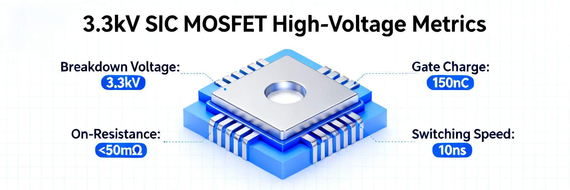
1.1 Key device specifications to extract from the datasheet
Point: Capture the datasheet fields that directly affect loss, reliability, and integration. Evidence: Manufacturer datasheets list Vds class, nominal voltage, typical Rds(on) at specified Tj, max Vgs, max Tj, die/package form, Ciss/Coss/Cgd, total gate charge Qg, and thermal resistances. Explanation: Record units (V, mΩ, nC, nF, °C, °C/W) and test conditions (Tj, Id, Vds, and gate-drive waveform) so bench comparisons match datasheet baselines.
1.2 Typical high-voltage applications and system-level constraints
Point: 3.3 kV-class SiC MOSFETs target HV inverters, traction drives, HV DC-DC stages and grid interfaces. Evidence: System architects require switching-frequency targets, insulation/creepage margins, and thermal budgets documented up front. Explanation: Map device metrics to system constraints: Rds(on) and thermal resistance limit continuous-current capability, switching energies drive cooling and EMI, and gate robustness informs isolation and driver choices.
2 — Core HV metrics explained (what to measure and why)
2.1 Electrical metrics to prioritize: Rds(on), Vth, gate charge, capacitances, switching energies
Point: Prioritize conduction and dynamic metrics that set loss balance. Evidence: Rds(on) at multiple Tj and Vgs, threshold Vth, Qg/Qgd, and capacitances (Coss, Crss) appear in datasheets and determine conduction vs switching trade-offs. Explanation: Report methods: DC Rds(on) sweeps at defined Tj and Id, and Qg measured with standardized gate-drive waveforms; quantify how each metric maps to conduction loss (I²Rds) and switching loss (Eon/Eoff).
2.2 Robustness and dynamic metrics: avalanche, SOA, thermal resistance, dv/dt ruggedness
Point: Reliability in HV systems depends on ruggedness metrics as much as steady losses. Evidence: Datasheets provide single-pulse avalanche energy, SOA boundaries, junction-to-case/ambient thermal resistance, and dv/dt limits. Explanation: Compare datasheet limits against expected transient stresses — e.g., fault energy during dc-link discharges — and use those margins to define derating and protection (short-circuit detection, snubbers).
3 — Measured performance: datasheet vs bench (how to present and compare results)
3.1 Conduction performance: Rds(on) vs temperature and implication on losses
Point: Present normalized Rds(on) curves to show temperature sensitivity and realistic conduction loss. Evidence: Bench DC sweeps and thermal bias tests from independent measurements should be plotted alongside datasheet curves. Explanation: Include Rds(on) at 25°C and elevated Tj (e.g., 125–175°C) and normalize to 25°C to compute I²R losses for expected duty cycles; beware contact resistance and Kelvin sense wiring in test setup.
| Parameter | Manufacturer datasheet | Independent bench |
|---|---|---|
| Vds rating (class) | ~3.3 kV | Verified ≥3.3 kV hold-off at low leakage |
| Rds(on) @ 25°C | e.g., 40 mΩ (typ) | Measured 42–46 mΩ (test current noted) |
| Qg (total) | e.g., 120 nC | Measured 125–135 nC (Vgs swing, test waveform) |
| Eon/Eoff @ Vbus | Spec curves | Double-pulse Eon/Eoff recorded per setup |
3.2 Switching performance: Qg/Qgd, Eon/Eoff, Coss and how they translate to switching loss
Point: Translate gate charge and energy into watts at target switching frequency. Evidence: Double-pulse switching-energy measurements and Coss vs Vds plots from bench tests show Eon/Eoff dependence on Vbus, gate resistor, and stray inductance. Explanation: Report switching energy normalized per device and per die area; document gate drive conditions (Vgs, Rg, measurement inductance) so loss models are reproducible across teams.
4 — Case study: integrating the MSC400SMA330D in a HV inverter module
4.1 System-level metrics: efficiency, thermal design, and EMI considerations
Point: Device-level numbers must be mapped to converter efficiency and thermal plan. Evidence: Using measured Rds(on) vs Tj and switching-energy curves, system simulations predict efficiency at selected switching frequency and load points. Explanation: Derive junction-to-ambient thermal budgets, estimate heatsink mass/area, and anticipate EMI mitigation (snubbers and common-mode filters) driven by dv/dt and Eoff profiles.
4.2 Practical layout and gate-drive choices used in the case
Point: Layout and gate-driver choices determine whether the device reaches datasheet performance. Evidence: Case uses minimized loop inductance, Kelvin source if package supports it, and gate resistances tailored for trade-offs between dV/dt control and switching loss. Explanation: Recommend gate Rg ranges, Miller mitigation techniques, and protection elements (RC snubbers, appropriately rated TVS or varistors) to protect against bus transients and limit Eoff spikes.
5 — Benchmarking & FOMs (how to compare MSC400SMA330D to peers)
5.1 Normalized figures-of-merit to use (Rds(on) * Qg, Eoss per V, thermal-capacity normalized)
Point: Use normalized FOMs to compare devices across die-area and voltage class. Evidence: Compute Rds(on)*Qg, Eoss per V, and thermal capacitance per mm² from datasheet and bench data. Explanation: Normalize per die area or package footprint and visualize with radar or normalized bar charts so trade-offs between conduction, switching, and thermal capacity are clear for system-level selection.
5.2 System-level comparison scenarios to report
Point: Tailor comparisons to realistic converter use cases. Evidence: Example scenarios: high-frequency traction converter (switching loss dominated), HV DC-DC at medium frequency (balanced losses), and low-frequency high-current stage (conduction dominated). Explanation: For each, prioritize different metrics and show expected efficiency and thermal outcomes, enabling engineers to choose the best FOM for the target application.
6 — Testing & validation checklist + design recommendations
6.1 Recommended test protocols and safety checklist
Point: Adopt standardized HV test protocols and safety practices. Evidence: Recommended tests include double-pulse switching-energy runs, DC Rds(on) sweeps at multiple Tj, thermal cycling, short-circuit timing, and controlled avalanche tests using proper energy-limiting. Explanation: Document instrumentation (high-speed probes, isolated gate drivers), bus inductance values, and safety interlocks; enforce creepage and clearance and secondary containment in HV labs.
6.2 Design and reliability recommendations (gate drive, derating, thermal management)
Point: Apply conservative derating and robust gate strategies to maximize lifetime. Evidence: Practical guidance: choose gate resistances to balance dV/dt and switching loss, derate Vds by specified margin against transient stress, and design heatsinking for worst-case junction temperatures. Explanation: Monitor early failure modes (parameter drift in Rds(on), threshold shifts) and apply periodic thermal cycling and margin testing in qualification.
Summary
- The MSC400SMA330D shows a balance of low conduction floor and controlled switching energy; validate manufacturer datasheet claims with DC Rds(on) sweeps and double-pulse switching tests to confirm real-world losses and thermal behavior.
- Key HV metrics—Rds(on) vs Tj, Qg/Qgd, Coss, Eon/Eoff, avalanche energy, and thermal resistance—determine converter efficiency, EMI needs, and required derating for reliable operation in 3.3 kV systems.
- Highest-impact design actions: tune gate drive (Rg and Miller mitigation), minimize loop inductance in layout, and size thermal management for worst-case junction temperatures to preserve lifetime and meet system efficiency targets.
7 — Frequently asked questions
What are the typical Rds(on) test conditions for MSC400SMA330D?
Datasheet Rds(on) is usually specified at a reference Tj (often 25°C) with a test current and Vgs. For bench parity, run DC Rds(on) sweeps with Kelvin sensing at the specified Id and repeat at elevated Tj to capture temperature coefficient; report wiring and contact resistance details for reproducibility.
How should MSC400SMA330D switching energy be measured for fair comparison?
Use a controlled double-pulse setup with documented bus voltage, known stray inductance, gate-drive voltage and gate resistor. Capture Eon and Eoff at representative Vbus and Rg values, and repeat at multiple inductances to understand sensitivity; normalize results per die area when comparing across devices.
What gate-drive and derating rules are recommended for MSC400SMA330D in a 3.3 kV inverter?
Recommend conservative derating of voltage and energy margins, select gate resistances that trade off dV/dt control and switching loss, and implement active protection (desaturation, fast short-circuit detection). Ensure thermal headroom through junction-to-ambient design and periodic qualification testing under thermal cycling.
Why is dV/dt transient ruggedness vital for 3.3 kV SiC MOSFETs?
High dV/dt switching transients can trigger parasitic turn-on through the Miller capacitance (Cgd), compromising gate oxide stability over time. Proper gate resistance tuning, Kelvin source layout routing, and negative turn-off gate bias prevent spurious turn-on and sustain component reliability.