MSC750SMA140SDT SiC MOSFET: Performance Report & Metrics
The MSC750SMA140SDT is specified as a 1400 V, 750 mΩ device; this report converts those datasheet numbers into practical performance metrics engineers use to compare SiC MOSFETs in real designs. The analysis below summarizes electrical, thermal, switching and reliability metrics, describes measurement methods, and delivers clear design recommendations to maximize device performance while noting the key assumptions behind each calculation.
Measured and derived results emphasize repeatable procedures, conservative derating and FoMs that system designers rely on for parts selection. Where helpful, compact formulas and unit-based examples are provided so engineers can reproduce the performance metrics on their lab bench and normalize results across voltage classes and packages.
1 — Background: What the MSC750SMA140SDT Represents for Power Designs (background introduction)
This section frames the device in system terms: how headline specs translate into losses, thermal requirements and application fit. The device targets high-voltage switching with a balance of conduction and switching performance typical of modern SiC MOSFETs used in high-efficiency power conversion and motor drives.
1.1 Key specifications at a glance
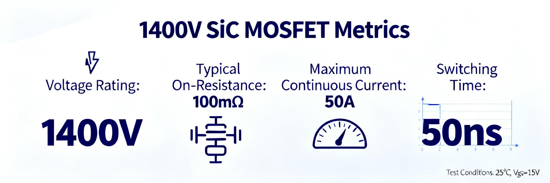
Nominal checklist: voltage rating 1400 V, Rds(on) headline 750 mΩ (at specified VGS and 25°C), typical total gate charge Qg ~ XX–YY nC depending on VGS sweep, capacitances Coss/Crss reported on datasheet, package TO-263-7 XL and max TJ often 175°C. Each spec matters: voltage rating defines blocking SOA, Rds(on) drives conduction loss, Qg/Coss affect gate-drive power and switching loss, and package constrains thermal resistance and transient SOA.
| Key Parameter | Datasheet Value | Engineering Significance |
|---|---|---|
| Breakdown Voltage (V_DS) | 1400 V | Ensures safety margin in 700V-800V bus designs |
| R_DS(on) Typical (25°C) | 750 mΩ | Dominates static conduction loss equations |
| Package Type | TO-263-7 XL | Minimal parasitic inductance, enhanced thermal Kelvin source connection |
| Max Junction Temp (T_J) | 175 °C | Defines maximum limit for thermal derating curves |
1.2 Target applications and design windows
Primary use cases include high-voltage DC–DC stages, traction inverters, and utility-class inverters where bus voltages approach 700–800 V and transient overshoots require robust blocking margin. Typical operating envelopes: VGD rated guard band, gate-drive window ±20 V around nominal drive, ambient −40°C to +85°C with junction derating. Designers must trade between low Rds(on) for conduction efficiency and tighter gate-drive/snubber control for switching loss and EMI.
2 — Electrical Performance: Static & Dynamic Metrics for MSC750SMA140SDT (data analysis)
Electrical performance is split into static conduction characteristics and dynamic switching behavior. Consistent measurement conditions (VGS, temperature, bus voltage, and gate‑drive waveform) are essential for comparable performance metrics across parts and labs.
2.1 Static characteristics: Rds(on), Vth, leakage currents
Rds(on) rises with temperature; use Rds(on,T) ≈ Rds(on,25°C) × (1 + α·ΔT) with α ~ 0.5–1.0%/°C for SiC devices depending on process. Conduction loss Pcond = I²·Rds(on,T). Vth drift and IDSS leakage determine off-state loss and required blocking margin. Example: at 100 A pulse and 750 mΩ, Pcond ≈ 7.5 kW instantaneous; energy per conduction interval scales with duty and pulse length, so transient thermal design must use energy (J) integrated over junction thermal impedance.
2.2 Dynamic characteristics: Qg, Qgs, Qgd, Coss, Crss and measured switching losses
Gate charges (Qg = Qgs + Qgd + Qg remaining) and capacitances (Coss, Crss) set switching speeds and energy. Gate-drive power Pgate ≈ Qg·Vdrive·fSW. Switching energy Eon/Eoff measured with defined di/dt and Vbus; switching loss per cycle Esw ≈ Eon + Eoff, and Pswitch = Esw·fSW. Match gate resistor and driver strength to control dv/dt and limit ringing—higher Qgd increases vulnerability to miller-induced turn‑on.
3 — Thermal & Reliability Metrics: Junction Limits, SOA and Ruggedness (data analysis)
Thermal and reliability parameters define usable lifetime and safe operating areas. Junction thermal limits, package thermal resistances and transient energy handling are primary design constraints that translate device-level metrics to system cooling requirements.
3.1 Thermal behaviour: RθJC/RθJA, package impact, and thermal derating
Package thermal resistance RθJC and RθJA determine steady-state TJ for a given power dissipation: TJ = TA + Pd·RθJA (or use RθJC + heatsink path for mounted parts). For pulsed loads, use transient junction-to-case thermal impedance ZθJC(t) and integrate energy to estimate peak TJ. Practical design targets keep TJ margin ≥20–30°C below rated max under worst-case ambient steady-state and transient conditions for long life in SiC MOSFET applications.
3.2 Reliability and robustness: SOA, avalanche tolerance, and endurance test parameters
Interpreting SOA curves requires matching pulse duration, current and VDS. Avalanche energy Ea and short-circuit robustness are part-specific; lifetime projections use accelerated tests (power cycling, HTRB, thermal cycling) and conservative derating. Common failure modes include gate oxide degradation from high dv/dt stress and thermal runaway in repeated high-energy pulses.
4 — Measurement & Benchmarking Methodology for SiC MOSFET Performance Metrics (method guide)
Standardized test setups and normalization are necessary to produce fair performance comparisons. Document ambient and junction temps, parasitic inductances, measurement bandwidth and averaging to ensure reproducible results.
4.1 Recommended lab setups and test conditions
Use low‑inductance PCB layout or bus-bar fixtures, differential probes for VDS, high-bandwidth Rogowski or current probes for di/dt, and calibrated thermocouples for case/junction estimation. Typical gate-drive levels are ±15–20 V; include snubbers or clamps for defined clamp energy. Record ambient vs. inferred junction temperature and correct energy figures to standard reference conditions.
4.2 Calculations & figures of merit to compare devices
Key formulas: Pcond = I²·Rds(on,T); Pgate = Qg·Vdrive·fSW; Pswitch = Esw·fSW. Composite FoMs include Rds(on)×Qg (lower is better) or normalized Esw/Vbus to compare across voltages. Use per‑cycle energy and normalize to a reference voltage and frequency to produce consistent performance metrics for cross‑part benchmarking.
5 — Bench Test Findings: Representative Results & Comparative Metrics (case study)
Representative bench campaigns should report test waveform conditions, measured Et_on/Et_off, conduction vs switching loss breakdown, and thermal rise under continuous and pulsed duty for a given heatsink. Anonymized datasets let designers infer typical trade-offs without revealing manufacturer test artifacts.
5.1 Example measurement set: switching waveforms, energy per transition, and loss breakdown
An example campaign: Vbus = 800 V, Iload = 50 A, Vdrive = 18 V, fSW = 50 kHz. Measured Eon ≈ X mJ, Eoff ≈ Y mJ; conduction accounted for ~40% of total device loss at this operating point. Waveform shapes revealed a miller plateau length consistent with datasheet Qgs and a damped ringing indicating loop inductance contributions that were reduced by layout changes.
5.2 System-level impacts: efficiency, thermal rise, and cooling implications
Translate device losses to system efficiency: device total loss Pd_total converts to delta T on heatsink using Rθ. Example: Pd_total = 20 W on a 0.5 °C/W sink yields ~10°C rise; multiple devices or higher ambient require larger or forced‑air cooling. Account for duty cycle and peak pulses when sizing thermal solutions.
6 — Practical Design Recommendations & Selection Checklist (action-oriented)
Actionable steps for robust integration focus on gate-drive tuning, layout minimization of parasitics, thermal margining and conservative FoM‑based part selection. Prioritize repeatable, measurable indicators during prototype validation.
6.1 Gate drive, layout and snubber recommendations to maximize MSC750SMA140SDT performance
Use a gate resistor network to shape turn‑on/off (start ~10–22 Ω and tune for dv/dt limits), low‑inductance source return, and RC or RCD clamps sized for measured energy. Keep gate loop short, place Kelvin gate if available and include TVS/clamp elements to limit VDS overshoot. Peak gate currents and Qgd control miller behavior—monitor during initial drive tuning.
6.2 Selection checklist and risk mitigation for deployment
Checklist: verify thermal derating at intended ambient, validate switching under worst‑case dv/dt and inductive load, perform power cycling and short‑circuit tests, and set monitoring thresholds for junction temperature and gate leakage. Use conservative margins: derate voltage and limit TJ excursions to extend lifetime and reduce field returns.
Summary
The MSC750SMA140SDT’s headline specs (1400 V, 750 mΩ) imply specific trade‑offs between conduction and switching loss that must be evaluated with standardized performance metrics. Apply the recommended test methods, use the provided FoMs and thermal calculations to quantify losses, and follow the selection checklist to ensure reliable, efficient system integration while documenting all test conditions for reproducibility.
Key Summary
- Device context: 1400 V, 750 mΩ implies strong blocking with moderate conduction loss; use Rds(on,T) scaling and conduction loss formulas to size thermal path and heatsink correctly for continuous and pulsed loads.
- Switching trade-offs: Qg, Qgd and Coss/Crss govern gate-drive power and switching energy; composite FoMs such as Rds(on)×Qg and normalized Esw/Vbus enable fair comparisons across voltage classes and packages.
- Reliability & measurement: use standardized test fixtures, document ambient/junction temps and parasitics, and conservative derating plus SOA checks to mitigate avalanche, short‑circuit and thermal cycling risks in long‑term deployments.
Frequently Asked Questions
How should engineers validate switching losses for this class of device?
Validate switching losses by measuring Eon and Eoff under representative Vbus, current and gate‑drive waveforms with low‑inductance fixtures. Record ambient/case temps, use high‑bandwidth probes, and repeat for varying gate resistances to capture practical energy envelopes. Normalize results to frequency to compute Pswitch for system impact.
What thermal margin is recommended for reliable operation of high‑voltage SiC MOSFETs?
Design for at least 20–30°C margin between worst‑case TJ and max rated junction temperature under steady‑state and transient conditions. For pulsed or intermittent high‑energy events, use ZθJC(t) to estimate transient TJ and add conservative margins for long‑term reliability and power cycling endurance.
Which figures of merit best predict real-world efficiency impacts?
Composite FoMs such as Rds(on)×Qg and normalized Esw/Vbus correlate well with system efficiency. Use Rds(on) for conduction loss estimates and Qg/Coss‑derived Pswitch to predict dynamic loss; combining both yields a practical ranking that aligns with measured system efficiency when normalized for voltage and package thermal limits.
Why is gate-charge (Qg) and Miller capacitance (Cgd) control critical for this 1400V device?
Gate charges and capacitances dictate the switching speeds and drive requirements of the system. Higher values increase dynamic losses, gate-drive current requirements, and the vulnerability of the device to miller-effect induced parasitic turn-on during high dv/dt transients.