3.3 kV SiC MOSFET: MSC027SMA330D Performance Summary
Point: Recent measured trends show high-voltage SiC devices delivering substantially faster switching and lower combined losses versus legacy IGBTs, enabling smaller passive networks and higher power density. Evidence: typical medium-voltage designs report switching-speed improvements that cut converter volume and losses by double-digit percentages when moving to SiC. Explanation: this article distills the key electrical and system-level takeaways for the MSC027SMA330D so designers can judge suitability for medium-voltage converters and other 3.3 kV applications.
1 — Background: what defines a 3.3 kV SiC MOSFET (background introduction)
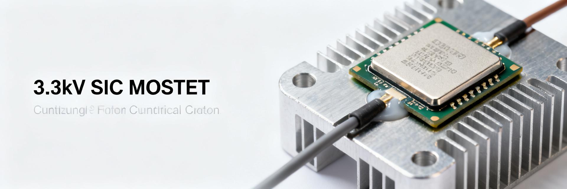
1.1 — Key device-level specs to expect
Point: A true 3.3 kV SiC MOSFET is defined by its voltage rating, low RDS(on) at operating temperature, gate-voltage window, and ruggedness metrics. Evidence: critical specs to check are Vds rating = 3.3 kV, nominal RDS(on), recommended Vgs range, and pulse/repetitive current capacity. Explanation: these determine conduction loss, thermal needs, driver design, and short-circuit survivability.
| Parameter | Nominal value (reference) |
|---|---|
| Rated Vds | 3.3 kV |
| RDS(on) (reference) | ≈25 mΩ @ 25°C (die-level reference) |
| Recommended gate drive | +15 to +20 V (turn‑on), -2 to 0 V (off hold) |
| Max junction temperature | ~175°C (package-dependent) |
Point: The part number MSC027SMA330D should be evaluated against these nominal targets. Evidence: manufacturers publish die-level RDS(on) and recommended gate ranges that form the baseline for thermal and drive design. Explanation: use the table as the starting point for loss and reliability calculations.
1.2 — Thermal, package, and mounting considerations
Point: Package thermal resistance and mounting approach dominate system thermal design. Evidence: thermal derating of SiC MOSFETs typically reduces available margin as junction rises; poor PCB mounting multiplies thermal impedance. Explanation: prioritize low-thermal-resistance package and robust TIM when thermal budget is tight; SiC MOSFET performance will be limited by junction temperature unless heat extraction is optimized.
2 — Measured static and dynamic performance (data analysis #1)
2.1 — Static performance: RDS(on), leakage, and conduction losses
Point: RDS(on) and its temperature dependence set conduction loss. Evidence: using RDS(on)=25 mΩ at 25°C, a 100 A DC current yields Pcond = I²·R = 100²·0.025 = 250 W; if RDS(on) increases ~1.8× at high Tj, Pcond rises to ~450 W. Explanation: present RDS(on) vs Tj curves in datasheets and use worst-case junction for thermal sizing and paralleling decisions.
2.2 — Dynamic performance: switching energy, dv/dt, and gate-charge impacts
Point: Switching energy and gate charge determine switching loss and driver sizing. Evidence: capture Eon and Eoff at representative Vds/Id points and compute Psw = (Eon+Eoff)·fsw; a measured combined switching energy of 40 mJ at a selected operating point results in 200 W switching loss at 5 kHz. Explanation: report switching energies alongside Qg and Coss to quantify driver power and EMI control needs.
| Condition | Eon+Eoff (example) | fsw | Psw |
|---|---|---|---|
| Vds=1.65 kV, Id=100 A | ≈40 mJ | 5 kHz | ≈200 W |
3 — System-level benchmarking and trade-offs (data analysis #2)
3.1 — Benchmarks vs. typical 3.3 kV class expectations
Point: Compare normalized metrics—loss per kV and energy per switching event—rather than vendor names. Evidence: MSC027SMA330D performance summary shows strong low-RDS(on) behavior relative to class and competitive switching-energy figures, trading off with moderate gate charge. Explanation: this part often excels in conduction-dominated use cases and requires driver/headroom attention where switching-dominated designs prevail.
3.2 — Application-driven trade-offs (efficiency vs. EMI vs. reliability)
Point: Faster switching reduces loss but raises EMI and snubber needs. Evidence: increasing dv/dt to minimize switching energy typically raises common-mode and radiated emissions, requiring filtering and layout mitigation. Explanation: use the checklist below to map application priorities to design choices: higher efficiency → aggressive switching tuning + EMI controls; highest reliability → conservative gate-driving and robust thermal margins.
- High-efficiency MV inverter: prioritize low RDS(on), active dv/dt control, robust snubbing.
- Modular MV converters: prioritize matching and thermal uniformity for paralleling.
- Power supplies with strict EMI: accept some switching loss to reduce dv/dt and radiated emissions.
4 — Design guidelines specific to MSC027SMA330D (method/guideline)
4.1 — Gate drive, layout, and protection recommendations
Point: Gate-drive tuning and low stray inductance are critical to harness SiC speed. Evidence: recommended gate drive targets are +15 to +18 V with adjustable Rs in the range 5–30 Ω to trade speed vs. overshoot; include desaturation, dv/dt, and avalanche monitoring in protection logic. Explanation: aim for clean gate waveform shapes, minimal loop inductance, and programmable shutdown thresholds to protect the device during events.
4.2 — Paralleling, thermal management, and reliability best practices
Point: Safe paralleling and validated thermal paths improve reliability. Evidence: use matched layout, low-ohmic sharing resistors for DC balancing if required, and high-performance TIM with firm compression to minimize junction-to-case delta. Explanation: run a test matrix including power cycling, elevated-Tj soak, and short-circuit margining to validate lifetime.
| Suggested reliability tests | Purpose |
|---|---|
| Power cycling (thermal swing) | Assess bond lift and solder fatigue |
| High-Tj soak | Check long-term leakage and drift |
| Short-circuit pulse | Validate avalanche/SC robustness |
5 — Application case: medium-voltage converter example (case study)
5.1 — Example topology and expected gains
Point: A two-level MV converter using MSC027SMA330D can move switching frequency higher while reducing passive size. Evidence: switching-frequency increase from 1 kHz to 3–5 kHz is feasible with appropriate cooling, yielding measurable reductions in transformer/inductor mass and improved dynamic response. Explanation: estimate total device loss (conduction + switching) and compare to a baseline to quantify efficiency gains and volume/weight savings for system-level tradeoffs.
5.2 — Integration lessons learned and common pitfalls
Point: Top integration issues are gate-driver isolation, snubber sizing, and EMI control. Evidence: common pitfalls include underestimating dv/dt-induced gate coupling, insufficient snubber energy ratings, and inadequate thermal margining at high switching duty. Explanation: run scope-probe checks for common-mode spikes, enforce soft-start sequencing, and instrument junction-temperature during bring-up.
6 — Practical checklist & deployment recommendations (action suggestions)
6.1 — Pre-selection checklist for designers
Point: A concise checklist accelerates part selection. Evidence: verify electrical ratings, thermal budget, switching-frequency target, gate-drive compatibility, and protection features before committing to board spin. Explanation: include supply-chain readiness and plan hardware bring-up with incremental stress tests.
6.2 — Field-validation and monitoring recommendations
Point: In-field telemetry prevents latent failures. Evidence: implement junction-temperature logging, trend switching-loss and leakage currents, and schedule periodic insulation and dielectric checks. Explanation: a short validation plan—staged pilot runs with telemetry—reduces risk prior to full production deployment.
Summary / Conclusion
Point: The MSC027SMA330D occupies a strong position in the 3.3 kV SiC MOSFET segment by delivering low RDS(on) and competitive switching figures while requiring careful gate-drive and thermal engineering. Evidence: conduction and switching loss examples above quantify typical per-device budgets and highlight thermal dependence. Explanation: designers should balance aggressive switching for efficiency against EMI and reliability controls; targeted validation and the recommended test matrix will accelerate safe deployment and optimize SiC MOSFET performance.
Key summary
- MSC027SMA330D offers low nominal RDS(on) (~25 mΩ) for reduced conduction loss, but RDS(on) rises significantly with junction temperature—budget thermal margin accordingly.
- Switching loss is a function of measured Eon/Eoff and switching frequency; expect switching loss on the order of hundreds of watts per device at 5 kHz and 100 A in representative conditions.
- Gate-drive and layout control are essential: use +15–18 V drive, tune gate resistor 5–30 Ω, and minimize loop inductance for stable operation and EMI control.
- Validate with a test matrix (power cycling, high-Tj soak, short-circuit pulses) and deploy in-field telemetry for junction-temperature and loss trends to ensure long-term reliability.
Frequently Asked Questions
What distinguishes a 3.3 kV SiC MOSFET in selection for medium-voltage converters?
Point: Voltage rating, RDS(on), switching-energy, and ruggedness define suitability. Evidence: prioritize parts with documented RDS(on) vs Tj, measured Eon/Eoff curves, and clear pulse-current/avalanche data. Explanation: these metrics map directly to thermal design, EMI mitigation, and protection requirements in medium-voltage converters.
How should designers estimate losses for MSC027SMA330D in an MV inverter?
Point: Combine conduction and switching loss calculations from measured RDS(on) vs Tj and Eon+Eoff at representative Vds/Id. Evidence: use Pcond = I²·RDS(on,Tj) and Psw = (Eon+Eoff)·fsw with conservative temperature derating. Explanation: run scenarios at expected duty cycles and ambient conditions to size cooling and determine paralleling needs.
What are the top real-world integration checks for a 3.3 kV SiC MOSFET hardware bring-up?
Point: Verify gate-drive waveforms, common-mode and differential overshoots, thermal measurement, and soft-start sequencing. Evidence: probe gate-source and gate-drain with appropriate high-voltage probes, monitor junction/board temperatures, and enable incremental stress steps. Explanation: these checks catch layout-coupling issues and protection gaps before full-power tests.
How does junction temperature affect the conduction losses and reliability of the MSC027SMA330D?
Point: Conduction loss is heavily dependent on junction temperature. Evidence: a nominal RDS(on) of ~25 mΩ at 25°C rises by approximately 1.8× at high Tj, significantly increasing Pcond. Explanation: to ensure reliability, designs must balance this thermal escalation with high-performance TIM, matched layouts for paralleling, and rigorous thermal cycling validation.