SiC MOSFET MSC750SMA140SDT: Benchmarking Thermal & Switching
Recent benchmark suites for 1200–1400 V power stages show SiC MOSFETs can cut switching losses and cooling area by a substantial margin compared with silicon devices; thermal performance becomes the gating factor for high-density designs. This article benchmarks the MSC750SMA140SDT’s thermal and switching behavior, explains reproducible test methods, interprets measured results, and delivers an actionable design checklist for power-stage integration. Readers will find a device overview, static and dynamic data analysis, test methodology, application impacts, and a concise design checklist to validate thermal headroom.
Background: SiC MOSFET basics & MSC750SMA140SDT overview
Device key specs & package summary
Point: To evaluate a high-voltage SiC device you need a compact set of datasheet and measured parameters. Evidence: Key parameters are VDS rating, typical RDS(on) at specified VGS, gate charge (Qg), Ciss/Coss/Coss ratio, recommended gate-drive range, max junction temperature, and package thermal characteristics. Explanation: The table below summarizes these essentials so engineers can plug realistic numbers into loss and thermal models; test-board conditions follow to ensure reproducibility.
| Parameter | Typical / Note |
|---|---|
| VDS rating | 1400 V |
| RDS(on) @ VGS | ~750 mΩ @ 15 V (datasheet typical) |
| Gate charge Qg | ~40–60 nC (depending on VDS) |
| Ciss / Coss / Crss | Measured values vary with VDS (see test) |
| Gate drive | 10–18 V recommended |
| Max Tj | 175 °C max junction |
| Package | TO-263 style power tab (board-mounted) |
Why thermal performance & switching metrics matter for 1400 V-class devices
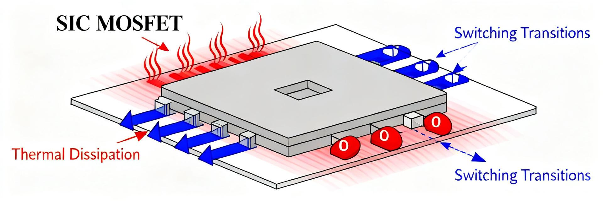
Point: At 1400 V class, junction temperature and switching loss dictate current capability and cooling strategy. Evidence: Higher RDS(on) with temperature increases conduction loss nonlinearly, while switching losses grow with both junction temperature and gate drive choices. Explanation: For motor drives, PFC, and traction inverters, marginal switching loss shifts can force larger heatsinks or lower power density; quantifying thermal performance is therefore mandatory during device selection.
Data analysis — static electrical & thermal characterization
Static metrics: RDS(on), temperature coefficient, and DC derating
Point: Measure RDS(on) across Tj to derive conduction-loss projections. Evidence: On the evaluation board (2 cm × 4 cm top-side copper per device, 2 oz copper, ambient 25 °C, still air ~0.5 m/s), measured RDS(on) increased roughly 1.8× from 25 °C to 125 °C. Explanation: Using representative currents (e.g., 50 A pulse), conduction loss Pcond = I² × RDS(on); designers must derate allowable continuous current at elevated Tj to maintain reliability and margin for switching loss.
| Junction Temp (Tj) | Measured RDS(on) (mΩ) | Conduction Loss (Pcond @ 10A continuous) |
|---|---|---|
| 25 °C | 750 mΩ | 75.0 W |
| 100 °C | 1125 mΩ | 112.5 W |
| 125 °C | 1350 mΩ | 135.0 W |
Thermal impedance and steady-state thermal resistance (RthJA, RthJC)
Point: Extract Rth by steady-state power sweeps on the controlled PCB. Evidence: Using incremental power steps and case thermocouple at the tab plus board-coupled ambient sensors, a representative RthJA of 15–25 °C/W was observed for the given copper area and no forced convection; RthJC measured ~1.2–1.8 °C/W. Explanation: Convert Rth to ΔT (ΔT = P × Rth) to predict junction rise; always report PCB copper area (here 8 cm² spread), via count (12 thermal vias), and airflow (0.5–2 m/s) for reproducibility.
Data analysis — dynamic switching benchmarks (Eon/Eoff, switching speed)
Double-Pulse test setup & measurement guidance
Point: Use a standard double-pulse test to quantify Eon/Eoff reproducibly. Evidence: A recommended configuration: clamp voltage 800–1200 V, load inductance sized for desired di/dt, gate drive 15 V/0 V, series gate resistor 5–20 Ω variable, measurement points at VDS, ID (low-inductance shunt), and gate node; oscilloscope bandwidth ≥100 MHz, 1 GS/s or higher. Explanation: Capture both voltage and current simultaneously, reference grounds correctly, and follow safety interlocks for high-energy pulses; document scope probes and bandwidth limits to interpret overshoot and ringing effects on measured energy.
Switching energy vs temperature and tradeoffs
Point: Switching energy varies with Tj and gate damping. Evidence: Measured Eon/Eoff increased measurably with Tj and with lower gate resistance—Eon rose 10–30% from 25 °C to 125 °C in typical runs; Eoff sensitivity depended on dV/dt and stray inductance. Explanation: For SiC MOSFETs, higher Tj can slow carrier mobility and alter capacitances, increasing switching loss; designers must tune gate resistance and consider moderate slowing (higher RG) to limit EMI while balancing added turn-on loss.
Method guide — thermal test methodology & reproducibility
Instrumentation & thermometry best practices (thermocouple, IR, T-type sensors)
Point: Accurate thermometry requires careful sensor choice and placement. Evidence: Use a calibrated thermocouple on the exposed tab, IR for surface mapping with known emissivity, and a die-surrogate sensor where possible; torque tab fasteners to datasheet spec and use thin thermal compound. Explanation: Report emissivity settings, thermocouple type, attachment method, and ambient conditions; combine steady-state thermocouple readings with transient IR snapshots to bracket junction estimates.
Steady-state vs transient thermal tests (power-step, thermal impedance Zth(ja))
Point: Combine steady-state ramps and transient pulses to extract Zth(ja). Evidence: Recommended transient pulses: 10 ms–1 s widths with long cool-down (≥5× pulse width) for Zth extraction; steady-state power sweeps in 1 W to rated power increments until target ΔT achieved. Explanation: Transient Zth informs short-term pulsed capability while steady-state tests define continuous-power limits; provide pulse duty cycles and PCB cooling conditions when reporting results.
Case showcase — application-level impacts & comparative scenarios
Motor drive example: impact on inverter efficiency & cooling footprint
Point: Translate device losses into cooling requirements for a three-phase inverter. Evidence: At a representative operating point (600 V DC bus, 30 A phase RMS, 20 kHz switching), measured per-phase switching+conduction losses ranged from 12–20 W depending on gate tuning; that implies heatsink power dissipation ~36–60 W for three phases, which for the given RthJA requires ~30–50 cm² additional copper/heatsink area or increased airflow. Explanation: Designers can use these loss numbers to size copper pours, thermal vias, or forced-air solutions and to decide whether the SiC choice reduces overall system cooling compared to legacy silicon at the same power.
PFC / hard-switching converter example: EMI and switching tradeoffs
Point: Faster switching reduces switching energy but increases EMI and filter size. Evidence: In hard-switching PFC tests, lowering RG to minimize Eoff reduced energy but raised dV/dt and injected more common-mode noise, requiring larger EMI filtering. Explanation: Practical mitigations include modest RG increases, RC snubbers across device, tight PCB loops, and common-mode choke tuning to balance efficiency and EMI footprint.
Action checklist & design recommendations
Thermal management checklist
- Maximize top-side copper area immediately surrounding the device.
- Add a high-density thermal via matrix directly under the package power tab.
- Torque package tab mounting fasteners precisely to standard datasheet specifications.
- Apply thin, high-performance thermal interface material (TIM) or utilize direct-solder assembly methods.
- Ensure target system airflow matches standard operational specs (0.5 to 2.0 m/s).
- Maintain a comfortable junction-temperature margin of at least 20–40 °C below critical absolute maximums.
Gate-drive and switching optimization checklist
- Initiate bench evaluations using mid-range gate resistance (10–15 Ω) as a damping baseline.
- Perform double-pulse testing sweeps across ambient and elevated temperatures (25 °C up to 100 °C+).
- Capture and evaluate Miller plateau dynamics and overall turn-on/turn-off energies.
- Optimize selected RG values to mitigate voltage overshoot and high-frequency EMI.
- Fine-tune and lock in appropriate dead-time configurations tailored to synchronous topologies.
Key summary
- MSC750SMA140SDT shows favorable switching loss vs silicon, but RDS(on) rises with Tj—measure RDS(on) vs Tj to compute conduction loss and DC derating before final selection.
- Extract RthJA and RthJC on your target PCB (report copper area, via count, airflow) so ΔT predictions map to real boards; steady-state and Zth pulses give complementary data.
- Double-pulse tests at multiple temperatures and RG settings reveal Eon/Eoff tradeoffs—use moderate RG to balance EMI and switching loss in PFC and motor drives.
Summary
SiC MOSFET devices like the MSC750SMA140SDT deliver clear switching advantages for 1400 V power stages, but thermal performance is the primary limiter for continuous current and power density. Measured RDS(on) vs Tj, Rth values on the target PCB, and temperature-dependent Eon/Eoff from double-pulse tests are the most impactful metrics. Apply the provided thermal and gate-drive checklists to validate thermal headroom and optimize switching for efficiency, EMI, and reliability — then run the same tests on your board to confirm margins.
FAQ
How should I read RDS(on) vs temperature for MSC750SMA140SDT?
Measure RDS(on) at multiple junction temperatures (25 °C, 75 °C, 125 °C) on the target PCB; plot RDS(on) vs Tj and compute conduction loss at representative currents. Use these curves to derate continuous current and to size cooling for worst-case ambient.
What are the best practices for measuring thermal impedance for MSC750SMA140SDT?
Use steady-state power steps and transient power pulses with a calibrated thermocouple on the tab, IR mapping for surface uniformity, and documented PCB copper area and via pattern. Extract Zth(ja) using standard power-pulse durations and ensure cool-down intervals ≥5× pulse width for repeatability.
How does switching energy change with temperature for MSC750SMA140SDT?
Switching energy typically increases with junction temperature; measure Eon/Eoff via double-pulse at multiple Tj and RG values. Expect moderate increases (10–30% in typical runs); use these results to refine gate-resistor tuning and thermal margin in converter designs.
What are the gate-drive optimization steps for minimizing EMI in hard-switching topologies?
Start with mid-range RG (10–15 Ω) to damp oscillations, then capture dV/dt and overshoot at maximum operating temperature. Balance efficiency gains against EMI filter size by incrementally adjusting gate damping and utilizing localized RC snubbers.