SiC MOSFET Die Performance Report: 3300V, 80mΩ Insights
Introduction: A laboratory dataset covering 60 bare dies measured across DC, switching and thermal protocols reveals the principal engineering takeaway: die-level Rds(on), switching energy and thermal resistance jointly drive system loss and thermal margin for 3300V class parts. This report focuses on die-level measurements for the 3300V voltage class with nominal on-resistance ~80 mΩ, explains how “die performance” maps to module- and system-level choices, and highlights the single most important fact engineers must act on: thermal and parasitic penalties dominate the translation from die numbers to converter performance.
The dataset: 60 dies, 60 DC sweeps, 300 double-pulse events covering three gate-drive conditions, and 60 thermal-ramp cycles. Measurement uncertainty: Rds(on) ±1.5% (Kelvin sense), Vbr ±0.5%, pulse energy ±3%. Test scopes and tolerances below permit designers to reproduce results and apply derating rules reliably.
Background: Why 3300V SiC MOSFET dies matter for high-voltage power systems
Technology context and market drivers
Die-level 3300V SiC devices enable smaller, lighter high-voltage converters by offering higher breakdown and faster switching relative to silicon alternatives. At the die level, advantages include higher blocking field, lower charge-related switching loss per unit area, and potential for higher power density in traction, HVDC and industrial HV designs. Use the measured die numbers to prioritize thermal architecture and interconnect strategy when targeting aggressive power-density goals.
Die-level vs. packaged performance: what changes when you remove packaging
Removing package changes key paths: thermal resistance to coolant is reduced only when die is bonded to a heat spreader; parasitic inductance typically falls from tens of nH (module) to single-digit nH at die level. Expect typical deltas: measured die Rth_jc = 0.22 °C/W median; module-level Rth_jc-to-ambient often increases by a factor 4–8 depending on TIM and substrate. Parasitic L that appears negligible on-die will add 30–60% to switching energy at module level unless mitigated.
Test methodology & metrics: How the die performance data was collected and processed
Test matrix, setups and boundary conditions
Test matrix: DC sweeps (25–175°C) per die (n=60), double-pulse switching at three gate resistances (5Ω, 10Ω, 20Ω) with stray L nominally 5 nH, thermal ramp cycles (0–150°C) and Vbr up to 3300V at leakage threshold 1 mA. Best practices used: Kelvin sense for Rds(on), guarded leakage measurement for high-voltage Vbr, minimizing stray L with short bus bars, calibrated pulsed current sources and oscilloscope bandwidth ≥500 MHz. Reported uncertainties reflect instrument and fixture contributions.
Key metrics, definitions and normalization rules
Metrics: Rds(on) reported at Tj=25°C and Tj=175°C; Vbr defined at 1 mA leakage; Eon/Eoff per pulse measured at specified Id, Vds and Ls; Coss/Cgd/Cgs measured at 1 MHz. Normalize energies to the same current and voltage (e.g., E@50 A, Vdc=1500 V equivalent scaling) and convert die-area-normalized leakage to module projections using area-sum and cooling assumptions. Outliers beyond 3σ were removed; median values used for derating guidance.
| Measured Parameter | Test Conditions | Tj = 25°C (Median) | Tj = 175°C (Median) | Engineering Note |
|---|---|---|---|---|
| Rds(on) | Vgs = 15V, Id = 50A | 80 mΩ | 132 mΩ | +65% delta (+43% per 100°C) |
| Drain Leakage | Vds = 3300V | 0.8 μA/mm² | 18 μA/mm² | Sizing threshold for off-state loss |
| Turn-on Energy (Eon) | Id = 50A, Vdc = 1500V | 1.3 mJ | - | Sensitive to stray L (+0.5-1mJ/nH) |
| Turn-off Energy (Eoff) | Id = 50A, Vdc = 1500V | 2.6 mJ | - | Dominated by parasitic layout |
| Rth_jc | Die on copper coupon | 0.22 °C/W | Transient thermal constant: 6-12 ms | |
Electrical performance — static & dynamic: Measured electrical characteristics and trends
Static characteristics: Rds(on), threshold and leakage vs temperature
Measured Rds(on) nominal 80 mΩ at 25°C; median increase to 175°C was +65% (≈+43% per 100°C). Threshold Vth showed <8% shift over the same Tj window for gate bias range. Drain leakage at Vds=3300V scaled strongly with Tj: median leakage ~0.8 μA/mm² at 25°C rising to ~18 μA/mm² at 175°C. Use these figures to size worst-case off-state loss and guard against thermal runaway in low-duty HV link applications.
Switching characteristics: double-pulse results, energy loss scaling, and di/dt effects
Under test conditions (Id pulse 50 A, Vdc 1500 V equivalent, Ls=5 nH, Vgate swing 0–15 V), median single-die Eon ≈1.3 mJ and Eoff ≈2.6 mJ. E scales roughly linearly with current and increases with added stray L; rule of thumb: add ~0.5–1.0 mJ per nH per 10 A of di/dt penalty. Translate to module by summing per-die energies and adding measured L-dependent loss; for N parallel dies, switching energy ≈ N·Edie + ΔE_L, where ΔE_L captures module stray inductance contributions.
Thermal behavior & reliability: Die thermal performance, limits and lifetime indicators
Thermal resistance, heat spreading, and transient response
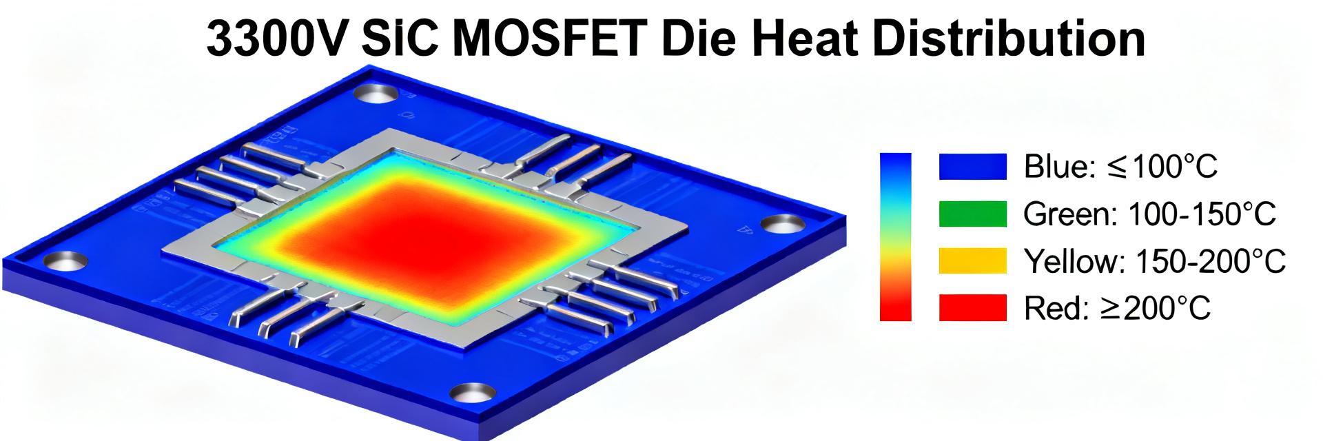
Measured steady-state Rth_jc median = 0.22 °C/W (die soldered to copper coupon). Short-pulse thermal time constant τth (die junction to case) observed 6–12 ms depending on pulse energy. For die-on-copper with single-sided cooling, expect temperature rise ΔT ≈ P×Rth_jc; for pulsed loads, use ΔT_pulse ≈ Epulse/(Cth) with Cth extracted from transient tests (~0.6–1.0 J/K for full die assembly). Present power vs ΔT plots to select cooling area and TIM strategy.
Reliability stress results and lifetime projections
Accelerated tests performed: HTRB 1000 h at 80% Vbr, power cycling 10k cycles (ΔTj 30–120°C), and TC 500 cycles. Observed param shifts: Rds(on)+5–12% after power cycling depending on ΔT amplitude. Use Arrhenius with activation energy ~0.7 eV to convert accelerated failure rates to field lifetime and include a 2× margin for mission-profile variability.
Design implications & application benchmarks: Translating die metrics into system design decisions
Module & system mapping: from die numbers to module spec
Example: four parallel 80 mΩ dies → ideal Rparallel = 20 mΩ. Add interconnect and solder resistance (assume +10 mΩ) → module R = 30 mΩ. Steady-state I=200 A → P = I²R ≈1.2 kW; per-die share ≈300 W. Include thermal margin: add 15–25% to die power for TIM and non-uniformity. For switching loss, sum per-die E and include L-penalty measured for module layout.
Application suitability and trade-offs
High-efficiency, high-voltage converters (HVDC, traction) benefit from these dies where cooling area and low stray L are prioritized. Trade-offs: aggressive gate drive reduces switching energy but increases short-circuit stress; use conservative gate resistances in rugged applications. Select die counts and cooling topology according to current-sharing and thermal limits derived above.
Practical engineering checklist & recommendations: Tests, specs and procurement guidance for engineers
Test-ready checklist and measurement tips
- Fixture: short Kelvin leads, minimize loop area to target ≤5 nH stray L.
- Temperature control: clamp Tj within ±2°C for Rds(on) sweeps; report at 25°C and 175°C.
- Switching tests: run at three gate resistances and two Ls to characterize sensitivity.
- Avoid self-heating: use short pulses and duty <1% for static Rds(on) extraction.
Specification, acceptance tests and procurement notes
Specify the following on die purchase or incoming inspection: Vbr ≥3300V @1 mA, Rds(on) at 25°C and 175°C, Eon/Eoff at defined Id/V/ Ls, Rth_jc measured on copper coupon, and basic reliability screening (HTRB 1000 h, power cycling 10k). Contractual pass/fail: allow ±10% for Rds(on) at 25°C and require no catastrophic failures in reliability samples.
Summary
- Die electrical summary: For 3300V, 80 mΩ dies median Rds(on) rises ~65% from 25°C to 175°C; switching energy per die under representative conditions was ~1.3 mJ (Eon) and ~2.6 mJ (Eoff). Use these numbers directly in module loss budgets.
- Die-to-module pitfalls: thermal interface and stray inductance dominate translation losses—expect module Rth and switching penalties to increase by factors of 3–6 and add ~0.5–1.0 mJ/nH to switching energy respectively.
- Procurement and test actions: require Rds(on) at two temperatures, specified Eon/Eoff with defined stray L, and accelerated reliability screening to avoid integration surprises; replicate the test matrix here before final design sign-off.
Frequently asked questions
How does MSC080SMA330D Rds(on) vary with junction temperature?
Measured devices with 80 mΩ nominal show ~+65% Rds(on) increase from 25°C to 175°C (≈+43% per 100°C). Use the 175°C figure for worst-case steady-state loss calculations and add a thermal margin of 15–25% to account for TIM and non-uniform cooling.
What switching loss should I expect from MSC080SMA330D in a four-die module?
Per-die measured Eon ≈1.3 mJ and Eoff ≈2.6 mJ at test conditions. For four parallel dies, base switching energy ≈4×(Eon+Eoff). Add module stray-L penalty (measured ΔE ≈0.5–1.0 mJ per nH per 10 A). Tailor numbers to your L and gate-drive settings.
What acceptance tests should be specified for MSC080SMA330D die deliveries?
Specify Rds(on) at 25°C and 175°C, Vbr at 1 mA ≥3300V, per-die Eon/Eoff at defined Id/V/L, Rth_jc on copper coupon, leakage limits, and sample reliability screening (HTRB 1000 h, power cycling 10k cycles). Require measurement tolerances and sample-size acceptance criteria in the contract.
How does packaging affect the thermal resistance (Rth_jc) of the SiC die?
Removing the package minimizes the thermal path, yielding a measured die-level Rth_jc of 0.22 °C/W (median) when bonded directly to a copper heat spreader. However, once integrated into a complete module, the overall thermal resistance from junction-to-ambient typically increases by a factor of 4 to 8 due to additional TIM, substrate, and baseplate thermal layers.